Substrate for light-emitting element and light-emitting device employing it
- Summary
- Abstract
- Description
- Claims
- Application Information
AI Technical Summary
Benefits of technology
Problems solved by technology
Method used
Image
Examples
first embodiment
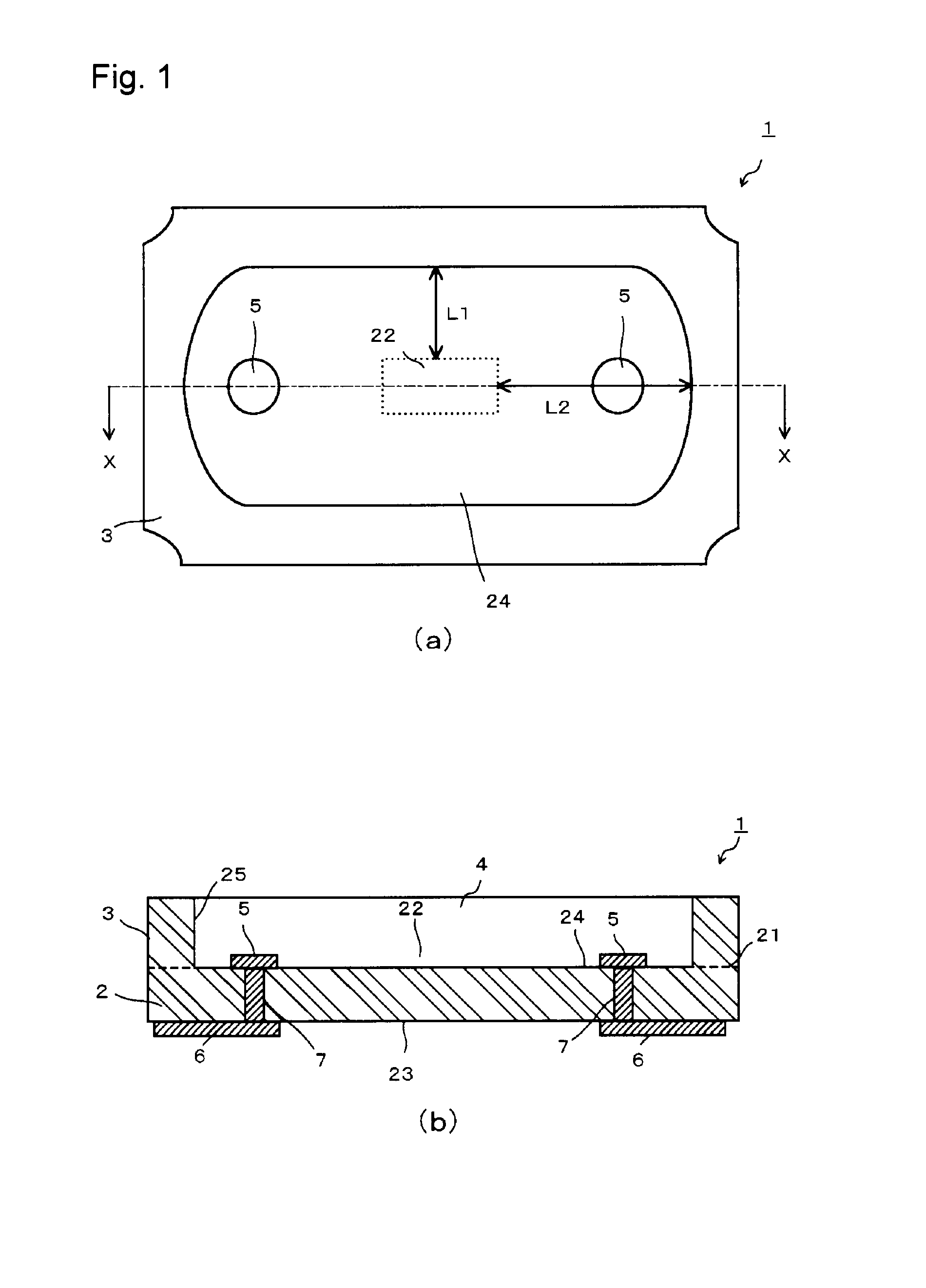
[0036]FIG. 1 is a plan view (a) illustrating an example of the substrate 1 for light-emitting element to mount one light-emitting element as the first embodiment of the present invention, and a cross-sectional view (b) along its X-X line.
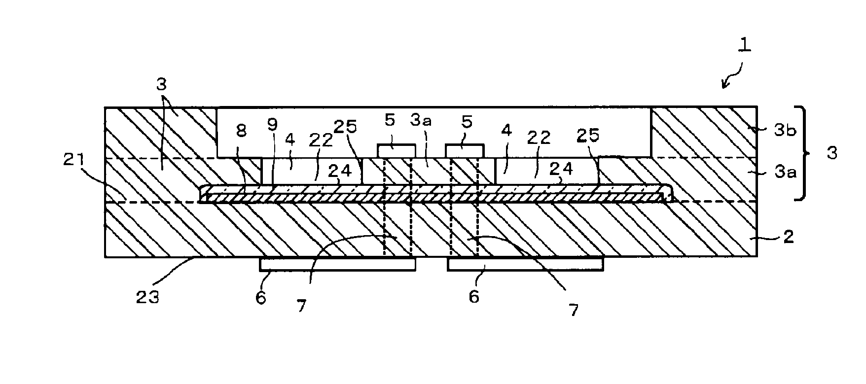
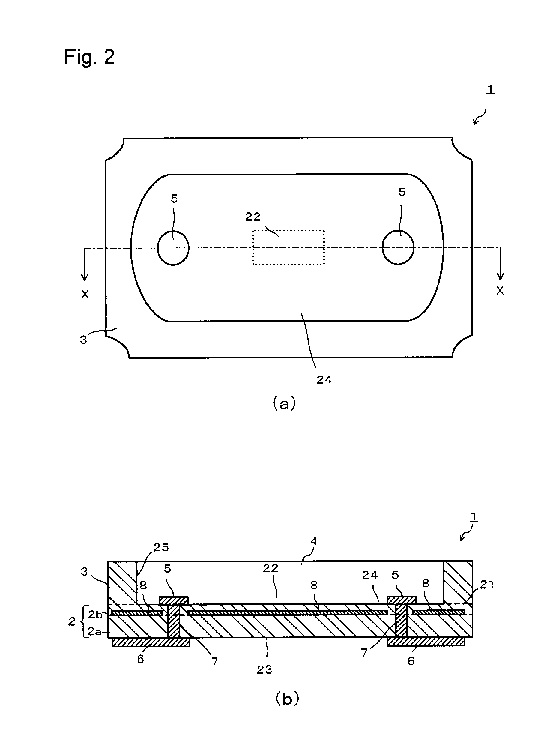
[0037]The substrate 1 for light-emitting element has a substantially flat-form base member having a substantially rectangular shape as viewed from above and mainly constituting the substrate. The base member 2 has the upper side surface as the main surface 21 on which a light-emitting element is to be mounted when used as a substrate for light-emitting element, and in this example, the opposite side surface is regarded as a rear surface 23. The substrate 1 for light-emitting element further has a frame member 3 bonded along the periphery of the main surface 21 of the base member to constitute a concave 4 having a bottom surface 24 constituted by a substantially rectangular portion at the center of the main surface 21 of the base member 2. Here, the ...
second embodiment
[0102]Now, as the second embodiment of the present invention, a substrate for light-emitting element to mount a plurality of light-emitting elements will be described.
[0103]FIG. 6 is a plan view (a) and a cross-sectional view (b) along its X-X line, illustrating an example of the substrate 1 for light-emitting element to mount plural, e.g. four, light-emitting elements as a second embodiment of the present invention.
[0104]The substrate 1 for light-emitting element according to the second embodiment of the present invention may, for example, be one on which, as shown in FIG. 7, four light-emitting elements 11 are to be mounted so that they are electrically connected in series at substantially circular positions in e.g. a quadrangular shape. In such a substrate 1 for light-emitting element, the light-emitting elements 11 are electrically connected in series by bonding wires 12, and a sealing layer 13 is provided to cover such light-emitting elements 11 and bonding wires 12, so that it...
example 1
[0147]By the following process, a light-emitting device for test was prepared wherein one light-emitting element 1 having the same structure as shown in FIG. 3 was mounted. Here, in the same manner as above, the same symbols are used for the components before and after the firing.
[0148]Firstly, a green sheet 2 for base member and a green sheet 3 for frame member were prepared to prepare the base member 2 and the frame member 3 for the substrate 1 for light-emitting element. For each green sheet, raw materials were blended and mixed so that SiO2 became 60.4 mol %, B2O3 15.6 mol %, Al2O3 6 mol %, CaO 15 mol %, K2O 1 mol % and Na2O 2 mol %, and this raw material mixture was put into a platinum crucible and melted at 1,600° C. for 60 minutes. Then, this molten state glass was cast and cooled. This glass was ground by a ball mill made of alumina to obtain a glass powder. Here, ethyl alcohol was used as the solvent at the time of grinding.
PUM
 Abstract
Description
Claims
Application Information
 - R&D
- Intellectual Property
- Life Sciences
- Materials
- Tech Scout
- Unparalleled Data Quality
- Higher Quality Content
- 60% Fewer Hallucinations
Browse by: Latest US Patents, China's latest patents, Technical Efficacy Thesaurus, Application Domain, Technology Topic, Popular Technical Reports.
© 2025 PatSnap. All rights reserved.Legal|Privacy policy|Modern Slavery Act Transparency Statement|Sitemap|About US| Contact US: help@patsnap.com


