Transistor and display device using the same

a technology of transistors and display devices, applied in the field of semiconductor elements, can solve the problems of delay in practical use, difficult to display images, and circuits formed using such transistors that do not operate normally, and achieve the effect of achieving advantageous effects

Active Publication Date: 2011-08-25
SEMICON ENERGY LAB CO LTD
View PDF7 Cites 25 Cited by
  • Summary
  • Abstract
  • Description
  • Claims
  • Application Information

AI Technical Summary

Benefits of technology

The patent text describes a method to reduce the impact of light irradiation on a transistor formed using an oxide semiconductor. The method aims to reduce the band tail state and defects in the band gap caused by light absorption. The technical effect of this method is to improve the stability and reliability of the transistor by reducing the effect of light irradiation and improving the performance of the display device or other electronic devices that use the transistor. The method involves removing impurities that form an impurity level in the oxide semiconductor by optimizing the manufacturing process and making the oxide semiconductor a substantially intrinsic semiconductor.

Problems solved by technology

In the oxide semiconductor of Patent Document 1 described above, when a transistor is irradiated with light having energy which is close to a band gap or higher than or equal to the band gap, it has been pointed out that the threshold voltage is changed by approximately 10 V. When the threshold voltage of the transistor is largely changed in this manner, a circuit which is formed using such a transistor does not operate normally, and it is difficult to display an image.
Any method for improving a change in characteristics, caused by such light irradiation, of a transistor formed using an oxide semiconductor is not proposed, which causes a delay in practical use while the oxide semiconductor is expected as a new material.

Method used


Image

  • Transistor and display device using the same
  • Transistor and display device using the same
  • Transistor and display device using the same

Examples


embodiment 1

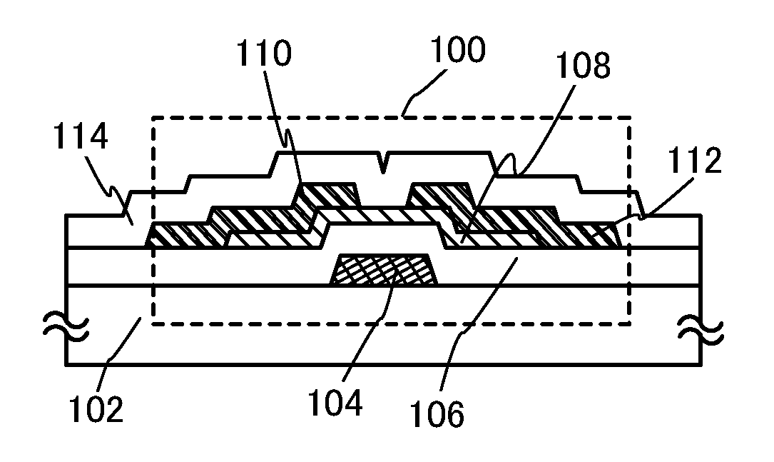
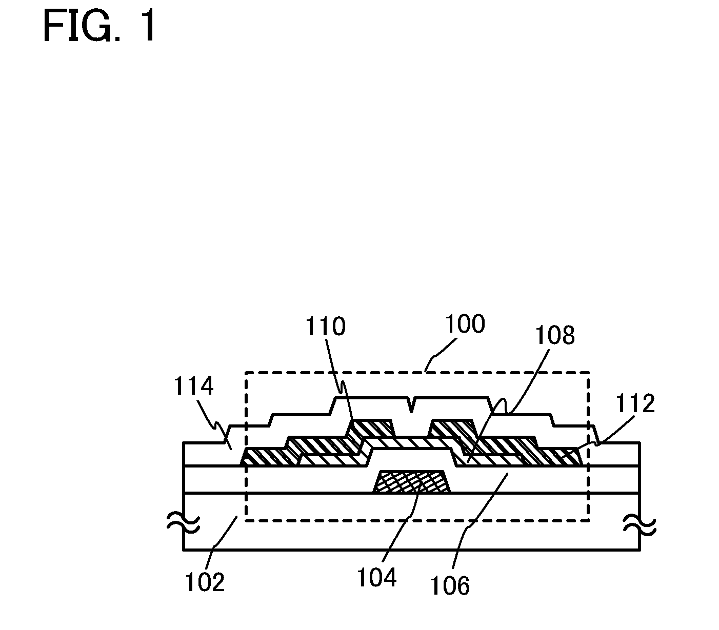
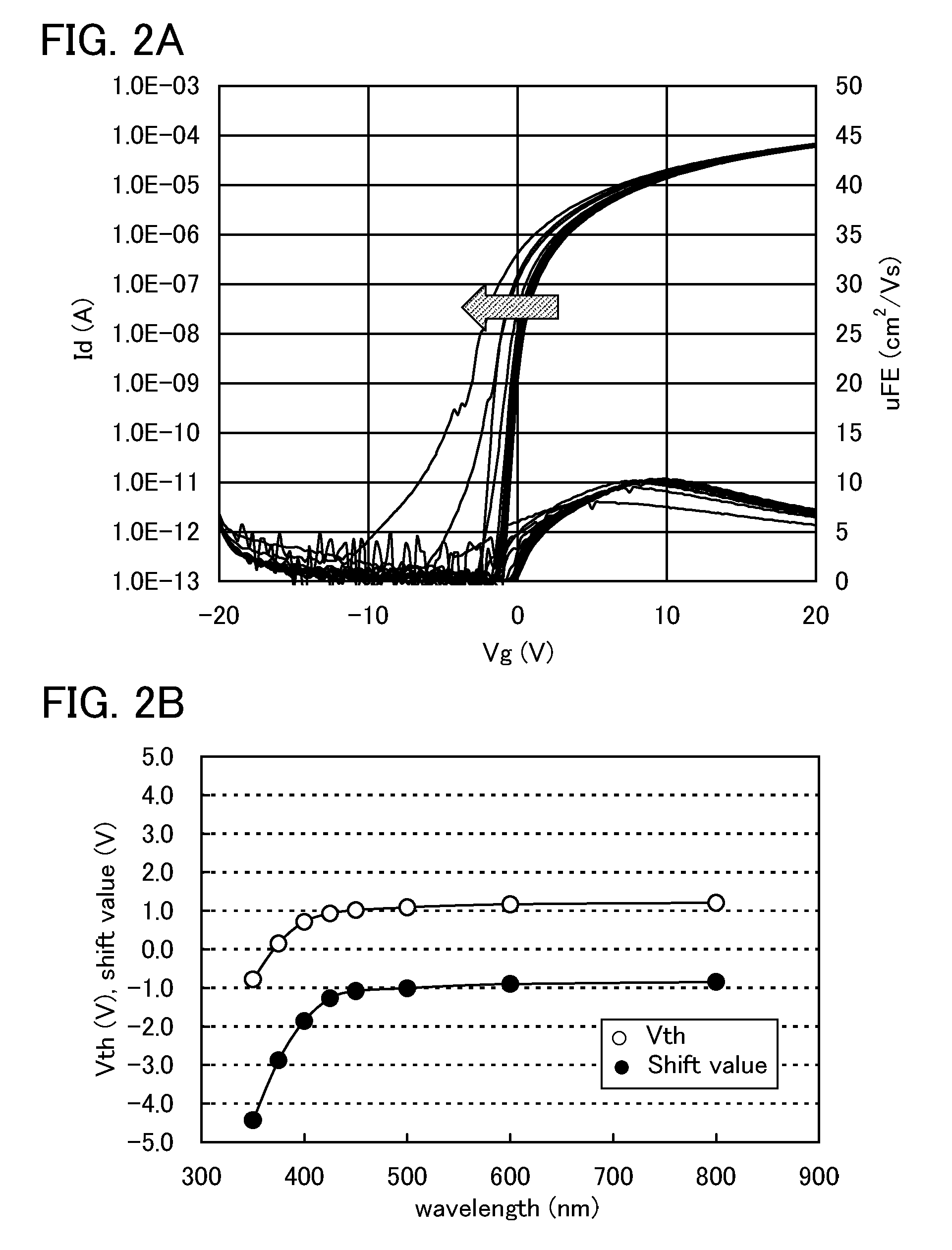
[0043]The structure of a transistor according to one embodiment of the present invention will be described with reference to FIG. 1, FIGS. 2A and 2B, FIGS. 3A and 3B, FIGS. 4A and 4B, FIGS. 5A and 5B, and FIG. 6.

[0044]A transistor 100 illustrated in FIG. 1 is a bottom-gate transistor and is also called an inverted staggered transistor. The transistor 100 includes, over a substrate 102 having an insulating surface, a gate electrode 104, a gate insulating layer 106, an oxide semiconductor layer 108, a source electrode 110, and a drain electrode 112. An insulating layer 114 is provided to cover the transistor 100 and be stacked over the oxide semiconductor layer 108.

[0045]The oxide semiconductor layer 108 is an intrinsic (i-type) or substantially intrinsic (i-type) oxide semiconductor layer which is obtained by removing hydrogen, moisture, or the like which is an impurity for an oxide semiconductor, and highly purifying the oxide semiconductor so that impurities which serve as carrier ...

embodiment 2

[0095]An example of a transistor having an operation effect which is similar to that of the transistor described in Embodiment 1 will be described with reference to drawings. The same portion as or a portion having a function similar to those in the above-described embodiment can be formed in a manner similar to that described in the above-described embodiment, and also the steps similar to those in the above-described embodiment can be performed in a manner similar to that described in the above-described embodiment, and repetitive description is omitted. In addition, detailed description of the same portions is not omitted.

[0096]When an oxide semiconductor in which the level in a gap and the band tail state are reduced is used, there is no particular limitation on a structure of a transistor in which the effect of light irradiation can be reduced. For example, a top gate structure in which a gate electrode is provided in the upper part of an oxide semiconductor layer with a gate i...

embodiment 3

[0143]A display device including the transistor an example of which is described in Embodiment 1 or Embodiment 2 can be manufactured. Moreover, some or all of the driver circuits which include the transistor can be formed over a substrate where the pixel portion is formed, whereby a system-on-panel can be obtained.

[0144]In FIG. 8A, a sealant 208 is provided so as to surround a pixel portion 202 provided over a first substrate 200, and the pixel portion 202 is sealed between the first substrate 200 and a second substrate 212. In FIG. 8A, a scan line driver circuit 206 and a signal line driver circuit 204 which are formed using a single crystal semiconductor film or a polycrystalline semiconductor film over a substrate separately prepared are mounted in a region that is different from the region surrounded by the sealant 208 over the first substrate 200. Various signals and potentials are supplied to the signal line driver circuit 204 and the scan line driver circuit 206 each of which...


PUM


Abstract

The band tail state and defects in the band gap are reduced as much as possible, whereby optical absorption of energy which is in the vicinity of the band gap or less than or equal to the band gap is reduced. In that case, not by merely optimizing conditions of manufacturing an oxide semiconductor film, but by making an oxide semiconductor to be a substantially intrinsic semiconductor or extremely close to an intrinsic semiconductor, defects on which irradiation light acts are reduced and the effect of light irradiation is reduced essentially. That is, even in the case where light with a wavelength of 350 nm is delivered at 1×10¹³ photons / cm2·sec, a channel region of a transistor is formed using an oxide semiconductor, in which the absolute value of the amount of the variation in the threshold voltage is less than or equal to 0.65 V.

Description

TECHNICAL FIELD[0001]The present invention relates to a semiconductor element such as a transistor and / or a display device at least part of which is formed using a semiconductor element. For example, an active element formed including an oxide semiconductor as a semiconductor element is illustrated, and a display device using the active element is illustrated.BACKGROUND ART[0002]Although transistors formed using amorphous silicon had been used for conventional display devices typified by liquid crystal televisions, an oxide semiconductor has attracted attention as a material which replaces a silicon semiconductor in order to form transistors. For example, an active matrix display device, in which an amorphous oxide including In, Ga, and Zn is used for an active layer of a transistor and the electron carrier concentration of the amorphous oxide is lower than 1018 / cm3, is disclosed (see Patent Document 1).[0003]However, some problems of a transistor formed using an oxide semiconducto...

Claims


Application Information

Patent Timeline
Patent Type & Authority Applications(United States)
IPC IPC(8): H01L29/786H05B44/00
CPCH01L29/7869H01L27/1225H01L21/42H01L27/156
Inventor TSUBUKU, MASASHINODA, KOSEI
Owner SEMICON ENERGY LAB CO LTD
Why Eureka
Try Eureka