
Photonic crystal enhanced light trapping solar cell

a solar cell and photonic crystal technology, applied in the field of high efficiency thin film solar cells, can solve the problems of limiting the usefulness of such cells to low electrical power applications or permanent applications, and one-junction silicon solar cells that capture less than half of the theoretical potential for solar energy conversion, etc., and achieves high efficiency.

Inactive Publication Date: 2011-08-25
UNIVERSITY OF DELAWARE
View PDF1 Cites 37 Cited by
  • Summary
  • Abstract
  • Description
  • Claims
  • Application Information

AI Technical Summary

Benefits of technology

[0008]This invention is directed to a high efficiency solar cell of a multi-layered structure...

Problems solved by technology

However, a one-junction silicon solar cell captures less than half of the theoretical potential for solar energy conversion with the best laboratory silicon solar cells currently providing only about 24.7% efficiency.
With such a low efficiency, large numbers of solar cells are required to generate electricity required for an application and this limits the usefulness of such cells to low electrical power applications or permanent applications wherein a large number of solar cells are used to supply sufficient electricity.
Many applications do not have the area required, for example, on the rooftops of domestic buildings or public or business buildings, to provide the needed power using current solar cells.

Method used


Image

  • Photonic crystal enhanced light trapping solar cell
  • Photonic crystal enhanced light trapping solar cell
  • Photonic crystal enhanced light trapping solar cell

Examples


Embodiment Construction

[0033]Definitions of terms as used herein:

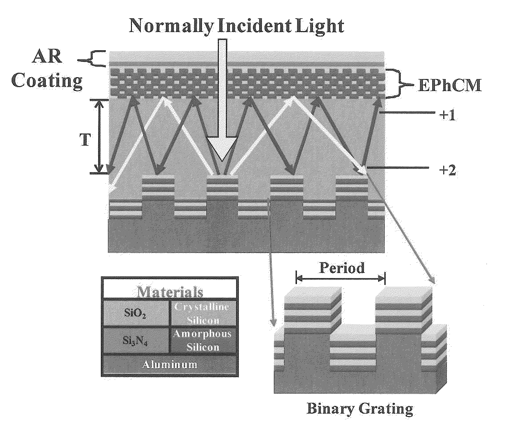
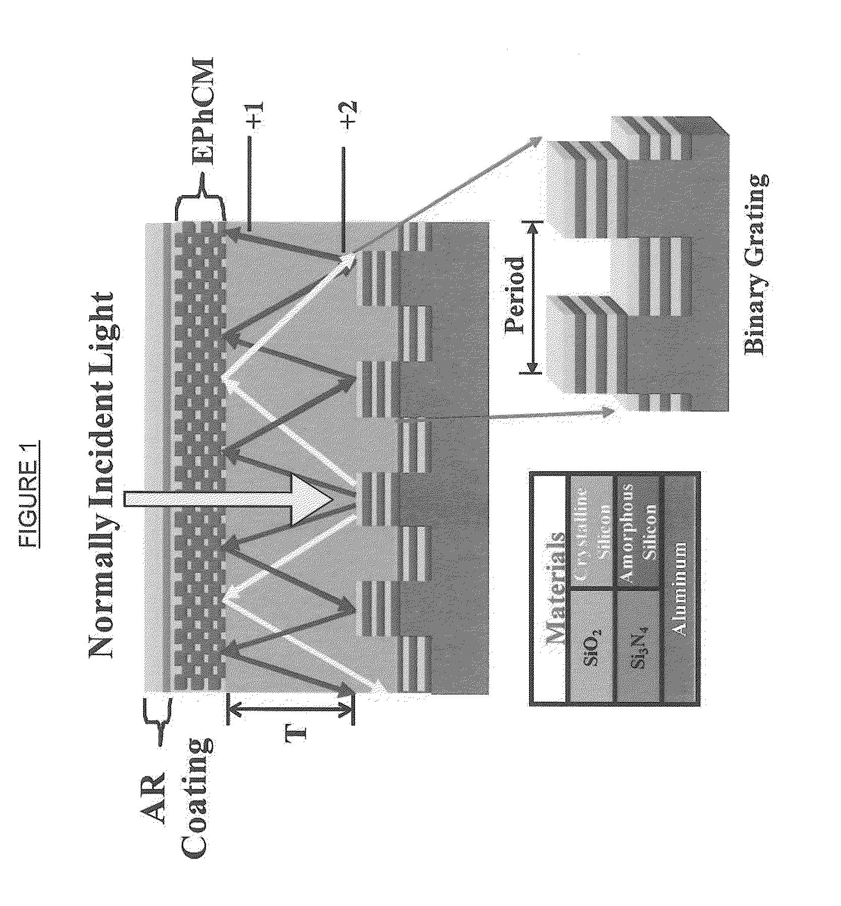
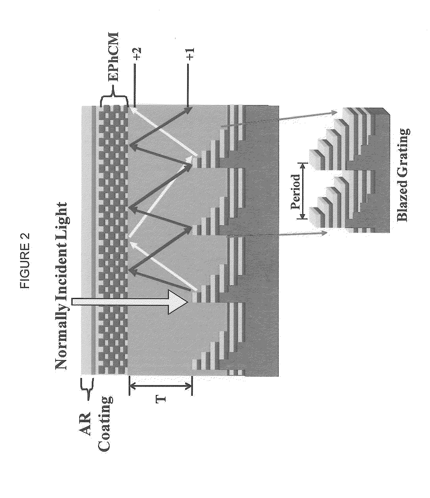
[0034]“AR Coating” means an anti reflective coating.

[0035]“c-Si” means crystalline silicon.

[0036]“a-Si” means amorphous silicon.

[0037]“EPhCM” means engineered photonic crystal material.

[0038]“PhCs” means photonic crystals.

[0039]“ID PhC” means one dimensional photonic crystal.

[0040]“2D-PhC” means two dimensional photonic crystal.

[0041]“3D-PhC” means three dimensional photonic crystal.

[0042]“Solar Cell” is used to describe the entire device.

[0043]“TFSC” means thin film solar cell.

[0044]“TIR” means total internal reflectance of a solar cell.

[0045]“Absorbed” as used herein, means that a photon absorbed by the cell results in the creation of an electron-hole pair and the energy of the photons is converted into electrical energy.

[0046]All percentages expressed herein are by weight of the total weight of the composition unless expressed otherwise.

[0047]Ranges are used herein in shorthand, to avoid having to list and describe each and every value wi...


PUM


Abstract

This invention relates to a high efficiency solar cell comprising: (a) a top surface of an anti-reflective coating layer; (b) an engineered photonic crystal material layer, (c) an active photovoltaic layer; (d) a photonic crystals with an integrated diffraction grating; (e) a metallic diffraction grating reflective layer, and (f) a metallic back reflector;whereby normally incident light striking the surface of the solar cell passes through the anti-reflective coating and the engineered photonic crystal material layer and is absorbed by active photovoltaic layer thereby generating electrical energy and obliquely incident light is reflected and diffracted by the engineered photonic crystal material layer, the one dimensional photonic crystal layer, the metallic grating reflective layer and the metallic back reflector to the active photovoltaic layer thereby generating electrical energy.

Description

CROSS REFERENCE TO RELATED APPLICATION[0001]This application claims the benefit of provisional application 61 / 306,605 filed Feb. 22, 2010 which is incorporated herein in its entirety.[0002]This invention was in part funded by the U.S. Government Defense Advanced Research Projects Agency under Agreement No.: HR0011-0709-0005. The Government has certain rights in the invention.FIELD OF THE INVENTION[0003]This invention relates to a high efficiency thin film solar cell that has an enhanced light trapping design and the solar cell is suitable for use in both mobile and stationary applications.BACKGROUND OF THE INVENTION[0004]The development of solar cells has been in progress for over fifty years. One-junction silicon solar cells have received much attention over that period and are used in terrestrial photovoltaic applications. However, a one-junction silicon solar cell captures less than half of the theoretical potential for solar energy conversion with the best laboratory silicon sol...

Claims


Application Information

Patent Timeline
IPC IPC(8): H01L31/0232
CPCH01L31/02168Y02E10/52H01L31/056B82Y20/00G02B6/1225G02B1/115G02B5/0808G02B5/09G02B5/1819G02B5/1861
Inventor PRATHER, DENNISSHI, SHOUYUANMUTITU, JAMESBARNETT, ALLEN
Owner UNIVERSITY OF DELAWARE
Learn More