Flash memory storage system, and controller and Anti-falsifying method thereof
a flash memory and storage system technology, applied in the direction of unauthorized memory use protection, memory adressing/allocation/relocation, instruments, etc., can solve the problems of system not being able to ward off falsification, data stored in the memory card is falsified by digital signature, and cannot be guaranteed in the integrity of data stored in the memory card, so as to prevent data stored in the flash memory chip from falsifying
- Summary
- Abstract
- Description
- Claims
- Application Information
AI Technical Summary
Benefits of technology
Problems solved by technology
Method used
Image

Examples
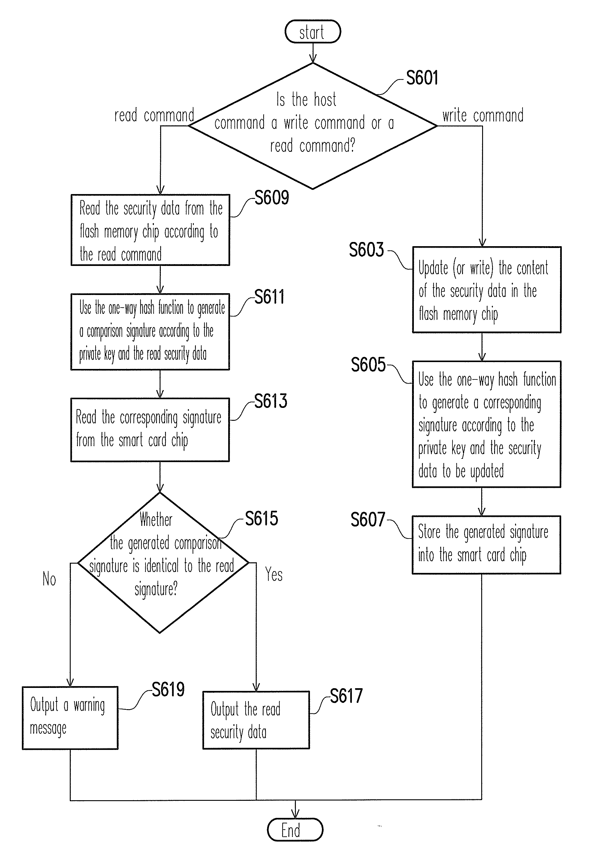
first exemplary embodiment
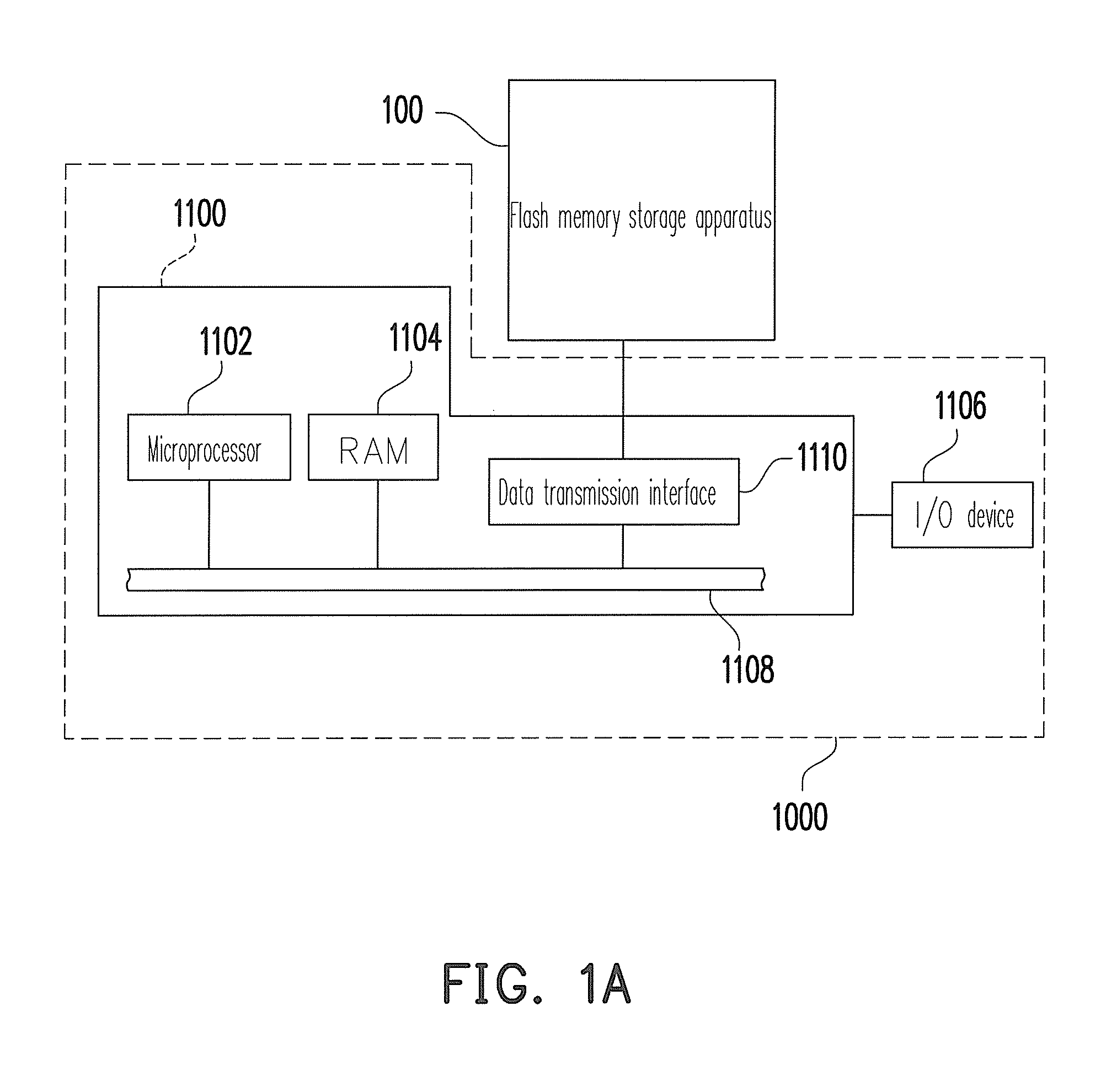
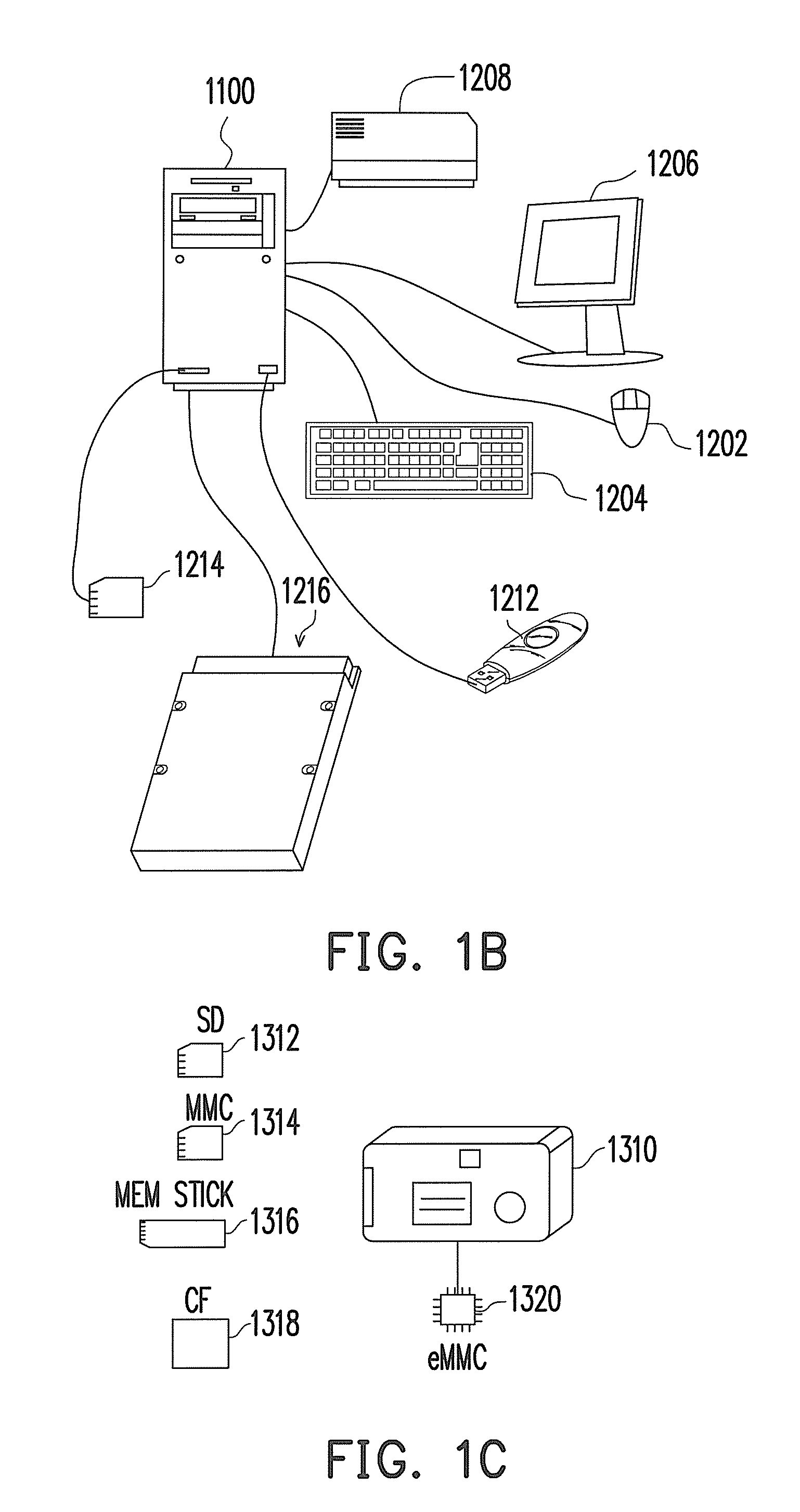
[0038]FIG. 1A is a schematic block diagram of a host system using a flash memory storage apparatus according to a first exemplary embodiment of the present invention. Referring to FIG. 1A, a host system 1000 includes a computer 1100 and an input / output (I / O) device 1106. The computer 1100 includes a microprocessor 1102, a random access memory (RAM) 1104, a system bus 1108, and a data transmission interface 1110. The I / O device 1106 includes a mouse 1202, a keyboard 1204, a display 1206, and a printer 1208, as shown in FIG. 1B. It should be understood that the devices illustrated in FIG. 1B are not intended to limit the scope of the I / O device 1106, and the I / O device 1106 may further include other devices.
[0039]In the exemplary embodiment of the present invention, the flash memory storage apparatus 100 is coupled to the devices of the host system 1000 through the data transmission interface 1110. By using the microprocessor 1102, the random access memory (RAM) 1104 and the Input / Out...
second exemplary embodiment
[0086]A flash memory storage apparatus and a host system in the second exemplary embodiment essentially are similar to the flash memory storage apparatus and the host system in the first exemplary embodiment, wherein the difference is that when a memory management unit updates security data, a security data protection unit stores an eigenvalue corresponding to the updated security data into a smart card chip and verifies the integrality of the security data based on the stored eigenvalue in the second exemplary embodiment.
[0087]FIG. 7 is a schematic block diagram illustrating a flash memory storage apparatus according to a second exemplary embodiment of the present invention. Referring to FIG. 7, the flash memory storage apparatus 700 is coupled to other devices of the host system 1000 through the data transmission interface 1110. By using the microprocessor 1102, the random access memory (RAM) 1104 and the Input / Output (I / O) device 1106, the data can be write into the flash memory ...
PUM
 Abstract
Description
Claims
Application Information
 - R&D
- Intellectual Property
- Life Sciences
- Materials
- Tech Scout
- Unparalleled Data Quality
- Higher Quality Content
- 60% Fewer Hallucinations
Browse by: Latest US Patents, China's latest patents, Technical Efficacy Thesaurus, Application Domain, Technology Topic, Popular Technical Reports.
© 2025 PatSnap. All rights reserved.Legal|Privacy policy|Modern Slavery Act Transparency Statement|Sitemap|About US| Contact US: help@patsnap.com