Programmable metallization cell with ion buffer layer

a metallization cell and buffer layer technology, applied in the direction of bulk negative resistance effect devices, electrical apparatus, semiconductor devices, etc., can solve the problems of poor data retention and cycling endurance, and achieve the effect of improving the retention of the conducting bridg

Active Publication Date: 2011-07-28
MACRONIX INT CO LTD
View PDF12 Cites 84 Cited by
  • Summary
  • Abstract
  • Description
  • Claims
  • Application Information

AI Technical Summary

Benefits of technology

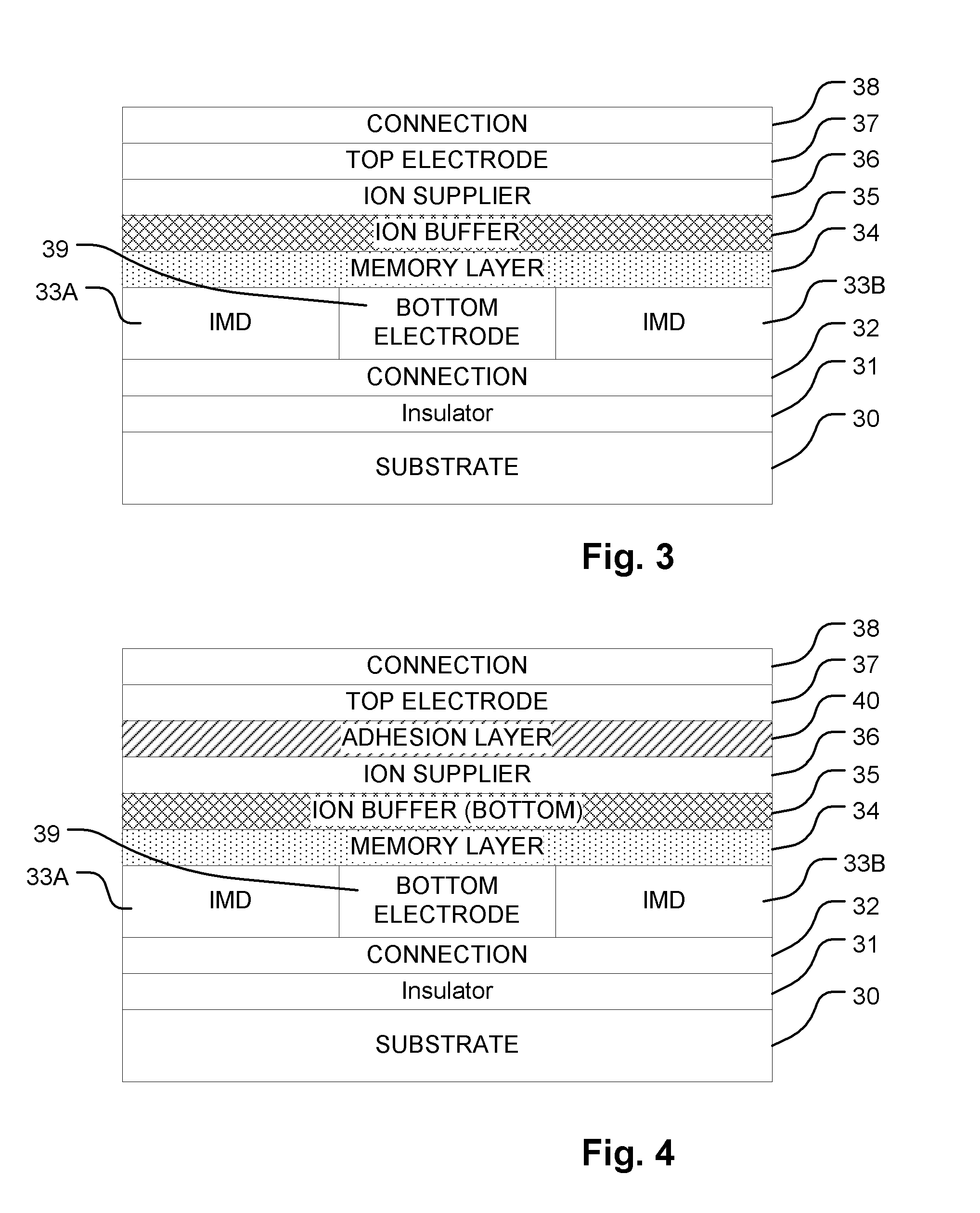
A programmable metallization device, comprises a first electrode; a memory layer electrically coupled to the first electrode and adapted for electrolytic formation and destruction of a conducting bridge therethrough; an ion supplying layer containing a source of ions of a first metal element capable of diffusion into and out of the memory layer; a conductive ion buffer layer between the ion supplying layer and the memory layer, and which allows diffusion therethrough of said ions; and a second electrode electric

Problems solved by technology

PMC devices, however, suffer from poor data retention and cyc

Method used


Image

  • Programmable metallization cell with ion buffer layer
  • Programmable metallization cell with ion buffer layer
  • Programmable metallization cell with ion buffer layer

Examples


Embodiment Construction

A detailed description of embodiments of the present invention is provided with reference to the FIGS. 1-10.

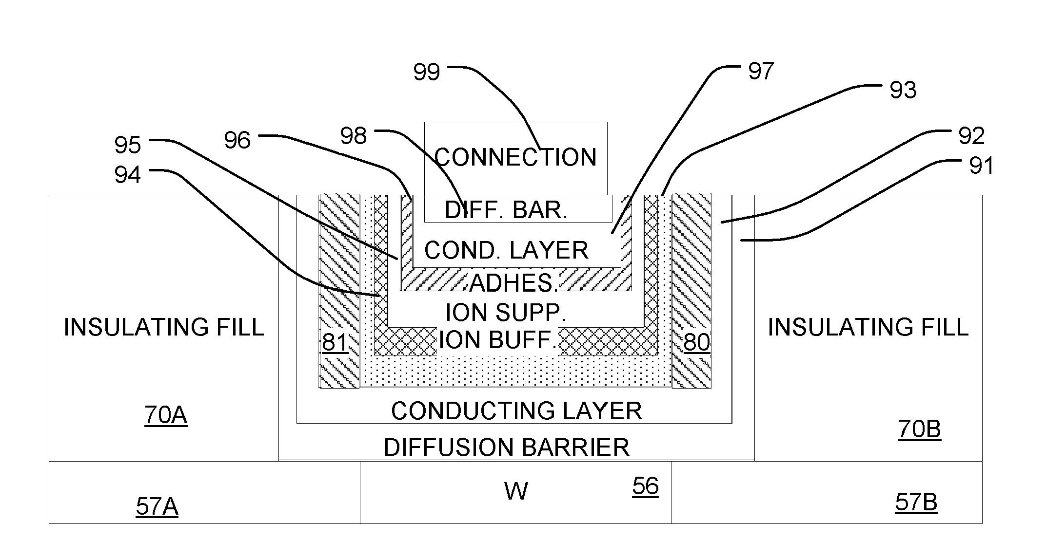
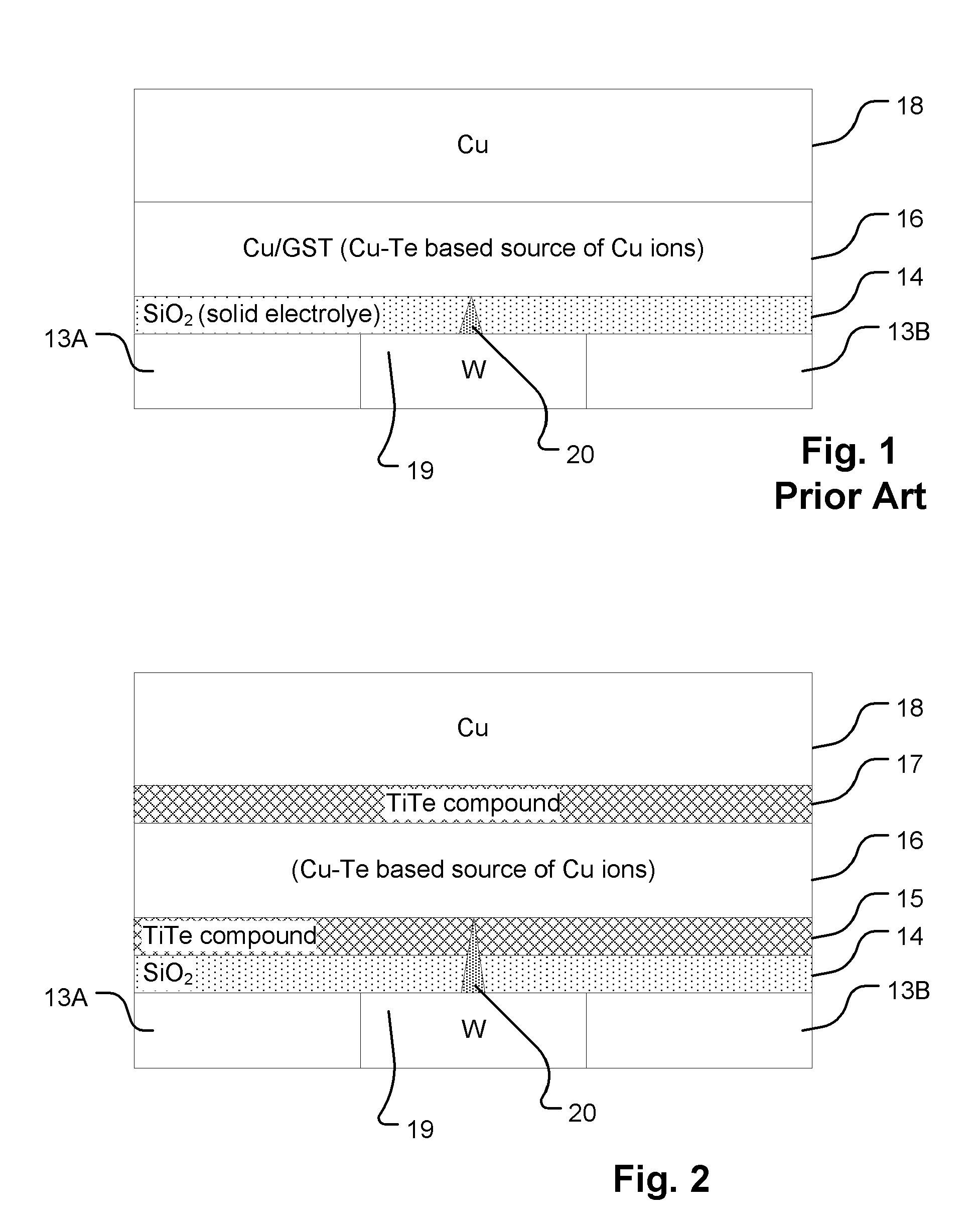
FIG. 1 illustrates a prior art PCM cell, as proposed by Aratani et al., “A Novel Resistance Memory with High Scalability and Nanosecond Switching,” IEEE International Electron Devices Meeting, 2007, 10-12 Dec. 2007, pp. 783-786. The cell in FIG. 1 is formed on an integrated circuit substrate that includes a dielectric layer (13A, 13B) with a tungsten contact 19 extending therethrough to provide a bottom electrode, and memory layer 14 of silicon dioxide, which acts as a solid electrolyte, is formed on the contact 19. An ion-supplying layer 16 of chalcogenide, such as Ge2Se2Te5, overlies the layer 14 of silicon dioxide, and includes a source of metal ions such as copper. In this composition, the copper can react with the tellurium in the chalcogenide to form a Cu—Te compound which readily dissolves to release copper cations. Thus the layer 16 (referred to as an ion activated lay...


PUM


Abstract

A programmable metallization device, comprises a first electrode; a memory layer electrically coupled to the first electrode and adapted for electrolytic formation and destruction of a conducting bridge therethrough; an ion-supplying layer containing a source of ions of a first metal element capable of diffusion into and out of the memory layer; a conductive ion buffer layer between the ion-supplying layer and the memory layer, and which allows diffusion therethrough of said ions; and a second electrode electrically coupled to the ion-supplying layer. Circuitry is coupled to the device to apply bias voltages to the first and second electrodes to induce creation and destruction of conducting bridges including the first metal element in the memory layer. The ion buffer layer can improve retention of the conducting bridge by reducing the likelihood that the first metallic element will be absorbed into the ion supplying layer.

Description

BACKGROUND OF THE INVENTION1. Field of the InventionThe present invention relates to programmable metallization cell technology.2. Description of Related ArtProgrammable Metallization Cell (PMC) technology for resistive switching is being investigated for use in nonvolatile memory, reconfigurable logic, and other switching applications due to its low current, good scalability, and high programming speed. The resistance switching of PMC devices is manifested by growing and removing conducting bridges through an electrochemical or electrolytic process. Therefore, PCM devices have also been referred to as conducting bridge CB devices or electro-chemical EC devices.PMC devices, however, suffer from poor data retention and cycling endurance because the conducting bridge can be unstable.SUMMARY OF THE INVENTIONA programmable metallization device, comprises a first electrode; a memory layer electrically coupled to the first electrode and adapted for electrolytic formation and destruction o...

Claims


Application Information

Patent Timeline
IPC IPC(8): H01L45/00H01L29/18H01L21/06
CPCH01L45/144H01L45/1266H01L45/122H01L45/085H01L45/1233H10N70/245H10N70/821H10N70/8416H10N70/883H10N70/826
Inventor LIN, YUYULEE, FENG-MINGCHEN, YI-CHOU
Owner MACRONIX INT CO LTD
Why Eureka
Try Eureka