Method for modifying a transparent electrode film
a technology of transparent electrodes and electrode films, applied in the direction of vacuum evaporation coating, electric/magnetic/electromagnetic heating, organic semiconductor devices, etc., can solve the problems of resin change in properties, deterioration of resin, and long time-consuming annealing, so as to reduce the resistivity of transparent electrodes and inhibit thermal deterioration and thermal distortion of substrates. , the effect of efficient annealing
- Summary
- Abstract
- Description
- Claims
- Application Information
AI Technical Summary
Benefits of technology
Problems solved by technology
Method used
Image
Examples
example 1
[0034]A substrate (material: glass, thickness: 0.7 mm) was introduced into a sputtering apparatus (manufactured by FTS Corporation, trade name “FTS (facing target sputtering) equipment”). A transparent electrode film (material: ITO, thickness: 150 nm) was formed on the surface of the substrate by a sputtering method under the following conditions, so that a transparent electrode film-attached substrate was obtained. The surface resistivity of the transparent electrode film in the obtained transparent electrode film-attached substrate was 51.7 Ω / square.
Film-forming pressure: 0.5 Pa
Ar flow rate: 40 scc / m
Oxygen flow rate: 0.5 scc / m
Input power: DC 1 kW
Film-forming rate: 11 nm / m
Target: ITO (10% by mass SnO2)
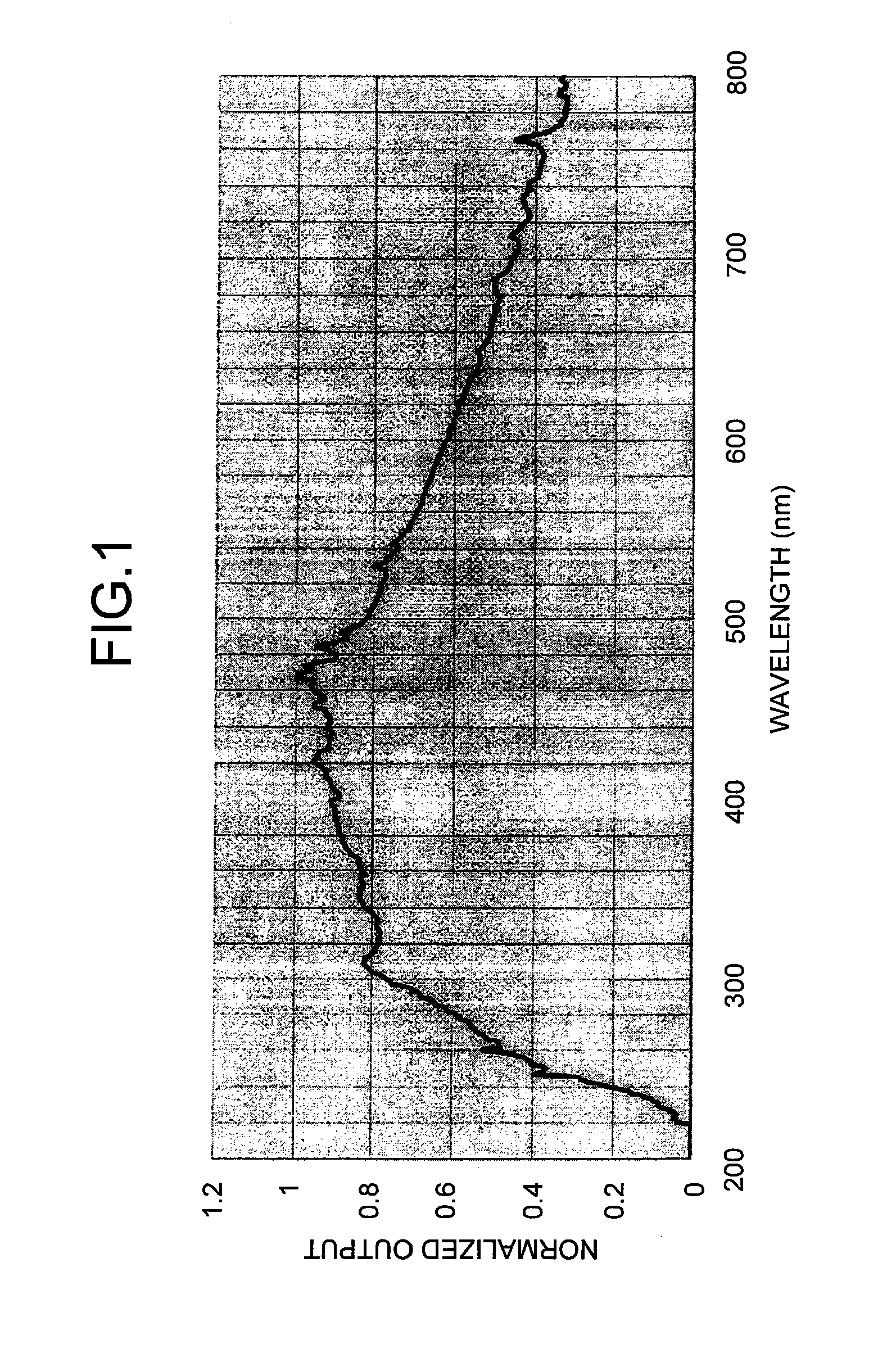
[0035]Flash light was then applied to the surface of the transparent electrode film of the obtained transparent electrode film-attached substrate using a flash annealing apparatus manufactured by USHIO INC. The transparent electrode film was annealed by a flash lamp, so that a transpa...
example 2
[0039]A transparent electrode film-attached substrate and a transparent electrode film-attached substrate that had been modified were obtained in the same manner as in Example 1, except that instead of that substrate (material: glass, thickness: 0.7 mm) a substrate made of a resin (material: polyethylene naphthalate, thickness: 125 μm) was used. The surface resistivity of the transparent electrode film in the transparent electrode film-attached substrate before modification was 53.2 Ω / square. The surface resistivity of the modified transparent electrode film in the transparent electrode film-attached substrate that had been modified was 18.4 Ω / square. The substrate made of a resin was not changed in shape and color. Therefore, according to the method of the present invention for modifying a transparent electrode film, it was confirmed that short-time annealing could sufficiently reduce the surface resistivity of a transparent electrode film. In addition, it was confirmed that the me...
PUM
| Property | Measurement | Unit |
|---|---|---|
| thickness | aaaaa | aaaaa |
| thickness | aaaaa | aaaaa |
| thickness | aaaaa | aaaaa |
Abstract
Description
Claims
Application Information
 - R&D
- Intellectual Property
- Life Sciences
- Materials
- Tech Scout
- Unparalleled Data Quality
- Higher Quality Content
- 60% Fewer Hallucinations
Browse by: Latest US Patents, China's latest patents, Technical Efficacy Thesaurus, Application Domain, Technology Topic, Popular Technical Reports.
© 2025 PatSnap. All rights reserved.Legal|Privacy policy|Modern Slavery Act Transparency Statement|Sitemap|About US| Contact US: help@patsnap.com

