
Metallization layer structure for flip chip package

a technology of flip chip and layer structure, which is applied in the direction of electrical equipment, semiconductor devices, semiconductor/solid-state device details, etc., can solve the problems of high cost of materials and equipment of gold-plating process, hard thickening or adhesion of film to ubm, and bottleneck in time consumed for wire-bonding technique, etc., to achieve easy fabrication, easy to shatter, and easy to peel off

Inactive Publication Date: 2011-06-23
NATIONAL TSING HUA UNIVERSITY
View PDF2 Cites 2 Cited by
  • Summary
  • Abstract
  • Description
  • Claims
  • Application Information

AI Technical Summary

Benefits of technology

[0009]The primary objective of the present invention is to provide an under-bump metallization layer, which is easy to fabricate, low-cost, tough, hard to peel off and corrosion-resistant.
[0011]Distinct from the conventional Au / Ni—P dual layer structure, the UBM layer of the present invention is a single NiZnP coated layer. Therefore, the present invention is easy to fabricate, low-cost, hard to shatter, and hard to peel off.

Problems solved by technology

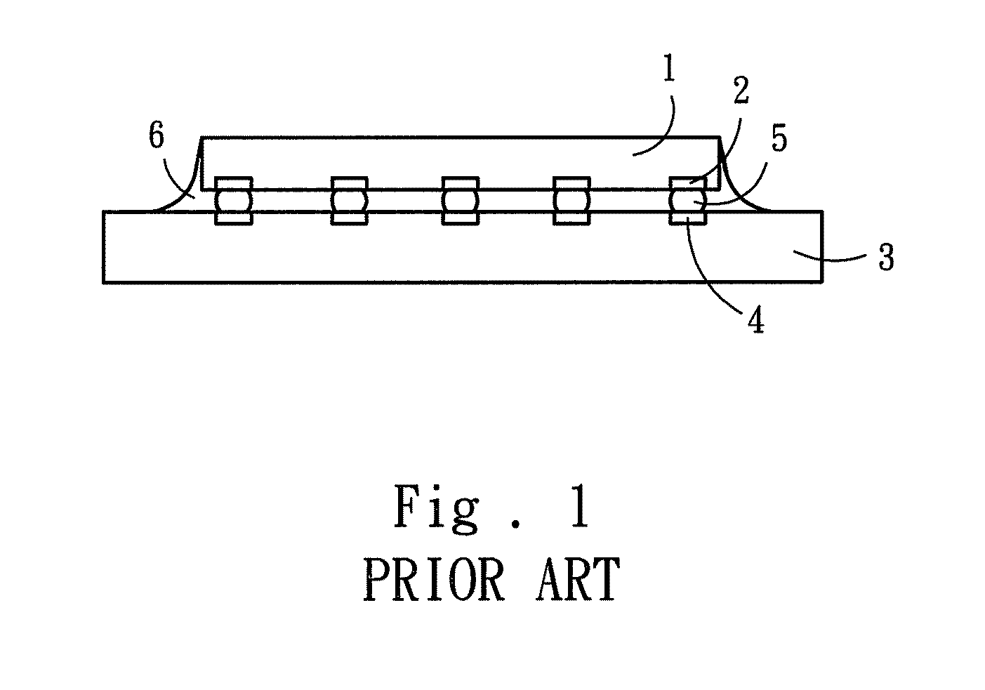
The wire-bonding technique has a bottleneck in the time consumed.
Further, the wire-bonding or the TAB technique packages greater volume electronic components, which conflicts with the current tendency to pursue slim and lightweight electronic products.
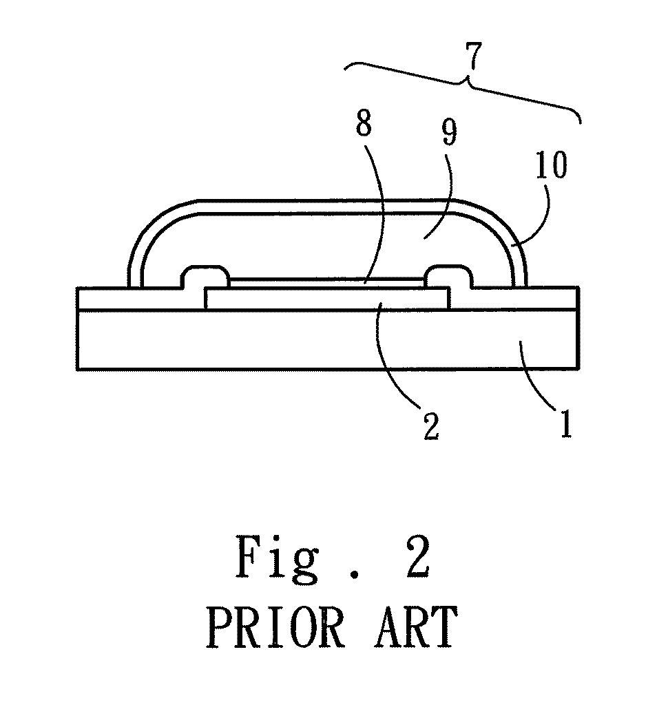
However, the materials and equipment of the gold-plating process is expensive.
Further, the gold film is hard to thicken or adhere to UBM 7 but easy to shatter or peel off.
Therefore, the gold-plating process has been a bottleneck of the F / C package process.

Method used


Image

  • Metallization layer structure for flip chip package
  • Metallization layer structure for flip chip package
  • Metallization layer structure for flip chip package

Examples


Embodiment Construction

[0017]The technical contents of the present invention will be described in detail with the embodiments. However, it should be understood that the embodiments are only to exemplify the present invention but not to limit the scope of the present invention.

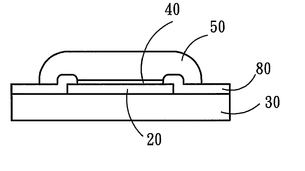
[0018]Refer to FIG. 3. The present invention proposes a metallization layer structure for flip chip package, which is formed on a metal pad 20. The metal pad 20 is formed on a chip 30. A passive protective layer 80 is also formed on the chip 30 to protect the chip 30, but the passive protective layer 80 exposes the metal pad 20. The metal pad 20 is made of a metal selected from the group consisting of aluminum and copper, which is usually used to form the connection points. The present invention comprises an UBM (Under-Bump Metallization) layer 50, which is a NiZnP coated layer formed on the metal pad 20.

[0019]The NiZnP UBM layer 50 can be formed via the reduction and oxidization of a solution containing nickel sulfate (Ni2SO4), zinc...


PUM


Abstract

The present invention discloses a metallization layer structure for flip chip package, which comprises an UBM layer formed on a metal pad, whereby a fine-quality tin-based solder ball can be formed on the metal pad. The UBM layer is a NiZnP layer formed via the reduction and oxidization of a solution containing nickel sulfate (Ni2SO4), zinc sulfate (ZnSO4), sodium dihydrogen phosphite (NaH2PO2), sodium citrate dihydrate (Na3C6H5O7-2H2O), and ammonium chloride (NH4Cl). The present invention replaces the conventional Au / Ni—P dual-layer structure. Therefore, the present invention can decrease the complexity of the process and reduce the cost. Further, the metallization layer structure of the present invention is tough, hard to peel off and highly corrosion-resistant.

Description

FIELD OF THE INVENTION[0001]The present invention relates to a structure for flip chip package, particularly to a metallization layer structure for flip chip package.BACKGROUND OF THE INVENTION[0002]In electronic package, the first stage packaging process, which connects a chip to a carrier, may be categorized into three package types, which are the wire-bonding technique, the TAB (Tape Automatic Bonding) technique, and the F / C (Flip Chip) bonding technique.[0003]The wire-bonding technique has a bottleneck in the time consumed. Further, the wire-bonding or the TAB technique packages greater volume electronic components, which conflicts with the current tendency to pursue slim and lightweight electronic products. Thus the F / C bonding technique was developed.[0004]The F / C bonding technique is to achieve high I / O pins, superior heat dissipation and compactness of an electronic package. Further, comparing with the wire-bonding technique, the F / C bonding technique greatly reduces the len...

Claims


Application Information

Patent Timeline
Patent Type & Authority Applications(United States)
IPC IPC(8): H01L23/485
CPCH01L2924/01011H01L2224/05124H01L2924/01015H01L2924/01022H01L2924/01029H01L2924/0103H01L2924/01074H01L2924/01078H01L2924/01079H01L2924/01006H01L2924/01024H01L2924/01047H01L2924/014H01L24/03H01L24/05H01L24/13H01L2224/05559H01L2224/05655H01L2224/13111H01L2224/05572H01L2924/01013H01L2224/05147H01L2924/00013H01L2924/0002H01L2224/0401H01L2224/13099H01L2224/13599H01L2224/05599H01L2224/05099H01L2224/29099H01L2224/29599H01L2924/00014H01L2224/05552
Inventor TAI, FONG-CHENGYU, CHI-YANGDUH, JENG-GONG
Owner NATIONAL TSING HUA UNIVERSITY
Learn More