[0010]The
beam shaping element and the laser diode chip always have the same temperature due to a temperature
control system with an appropriate temperature control. This can be achieved with a Peltier element, an actual
heating system, or a combination of
heating system and Peltier element. In this way, especially the laser aperture of the laser diode chip and the boundary surface of the beam shaping element associated with the aperture have a uniform temperature. With surface-to-surface
contact type connections, due to the identical temperature of the laser diode chip and of the lens or the concave mirror, no uncontrollable mechanical stresses will occur that might impair the reliability of the laser diode structure. Due to the connection, without spacing, of the laser aperture and the beam shaping element, the danger of a reflection of part of the
laser light of the laser beam on the boundary surface of the beam shaping element that faces the laser aperture is significantly reduced.
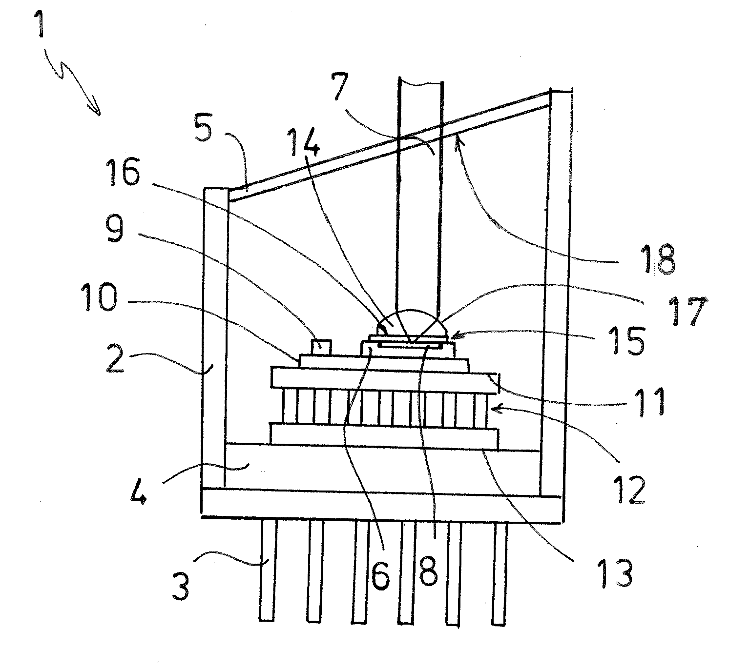
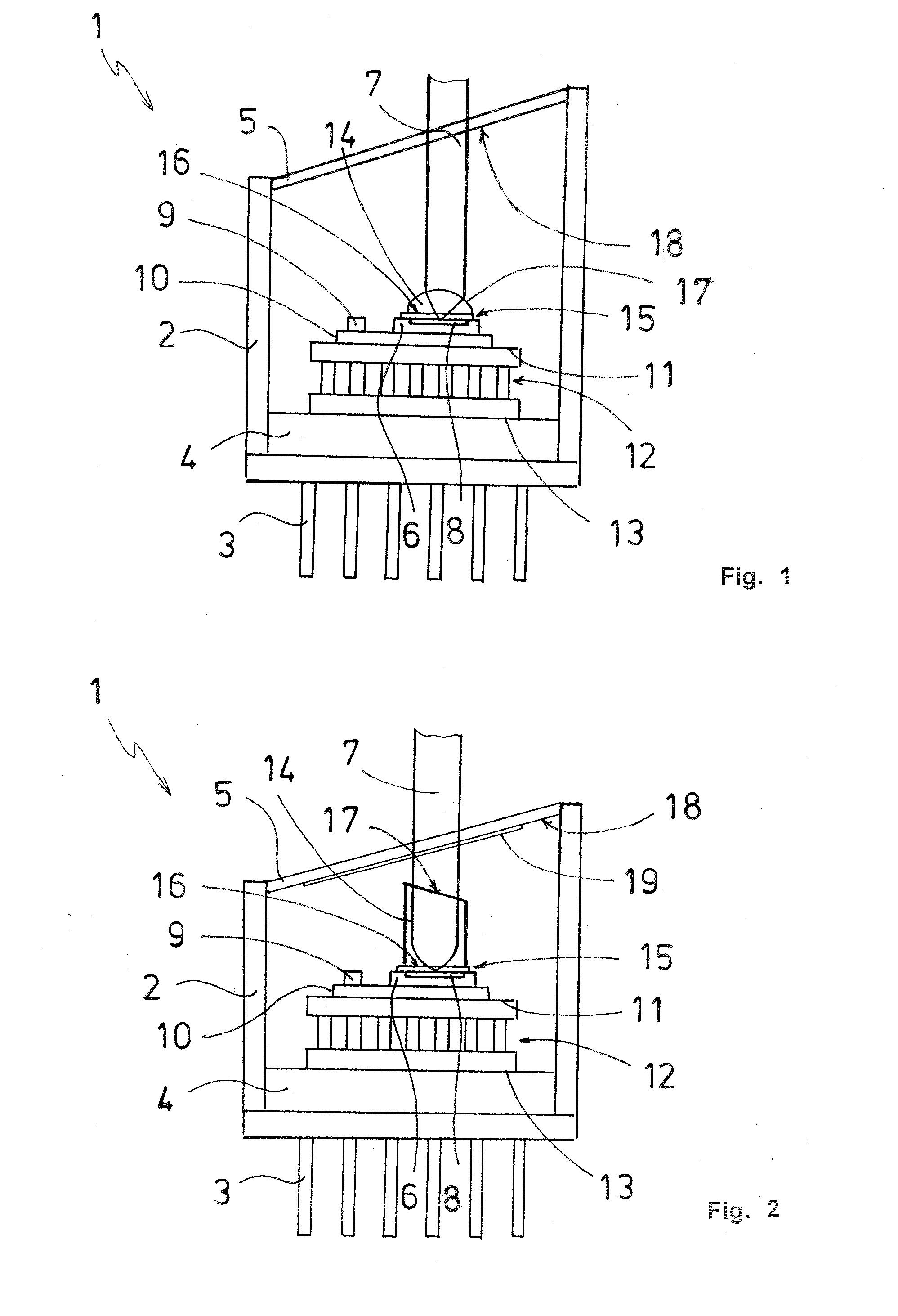
[0013]In order to prevent
stray light in the housing of the laser diode structure due to bending of the laser beam at the transition from the laser diode chip to the beam shaping element, where such
stray light can be reflected back in the direction of the laser aperture, parallel to the laser beam emerging from the laser diode chip, it is an
advantage if the boundary surfaces of the beam shaping element and of the laser aperture of the laser diode chip are uniform in terms of shape and size. Then, the
aperture angle of the laser beam emerging from the laser aperture corresponds to an aperture of the beam shaping element. It is obvious that the boundary surface of the beam shaping element facing the laser aperture may also be made larger than the laser aperture of the laser diode chip, and that the shape of the boundary surface may also deviate from the shape of the laser aperture, as long as it completely covers the laser aperture.
[0014]It proved to be especially advantageous to select an
adhesive agent for connecting the beam shaping element to the laser aperture that has a
refractory index that corresponds to that of the beam shaping element. By the uniform
refractory index of the
adhesive agent layer and the beam shaping element, the
compound system consisting of laser diode chip,
adhesive agent layer, and beam shaping element is reduced to a single light-refracting boundary surface between these. The effective boundary surface is located between the laser aperture and the adhesive agent layer. The boundary surface of the beam shaping element facing the laser diode chip and the adhesive agent layer is suppressed so that, from its emergence from the laser diode chip until it emerges from the beam shaping element, the laser beam is refracted only a single time at the transition between the laser aperture and the adhesive agent. This also eliminates a possible reflection surface for the laser light in the housing of the laser diode structure.
[0017]Ideally, the
microlens or the GRIN lens has a plane boundary surface associated with the laser aperture. In principle, concave boundary surfaces are also possible if they are leveled by the adhesive layer. With the
microlens specified above, the laser light moves in a straight line in the lens due to the homogeneous
refractory index of the lens material while, with a GRIN lens, it moves along a curved path in the lens due to the inhomogeneous refractory index. In a GRIN lens, there usually is a square-law decrease of the refractory index with the distance to the center axis (parabola function). A rod made of such a material acts like a common convergent lens but usually has plane surfaces at the light entry and light exit sides. This simplifies the
assembly, the
miniaturization, and the connection to the subsequent optical elements.
[0023]The invention offers the
advantage that because of the collimated laser beam not hitting the window perpendicularly, reflections possibly occurring on the window are not superimposed on the laser beam directed at the window so that interference phenomena of the laser beam inside the laser diode structure are reliably avoided. It also has the
advantage that, due to the temperature-controlled beam shaping element that is connected with the laser diode chip in a thermally conductive way, no significant temperature differences will occur so that the beam shaping element has no negative effects on the etalons. In addition, due to a reduction of the transitions of the laser beam in the housing from an optically more dense to an optically less dense medium or vice versa, the number of reflections occurring on boundary surfaces is reduced. This significantly increases the detection limits of a gas sensor as well as its reliability compared to known laser diode structures. Also, the manufacture of a laser diode structure is cost-efficient, with the additional costs compared with conventional laser diode structures being small.
