
Calibrated wideband high frequency passive impedance probe

Inactive Publication Date: 2011-05-05
AESTECH
View PDF19 Cites 9 Cited by
  • Summary
  • Abstract
  • Description
  • Claims
  • Application Information

AI Technical Summary

Benefits of technology

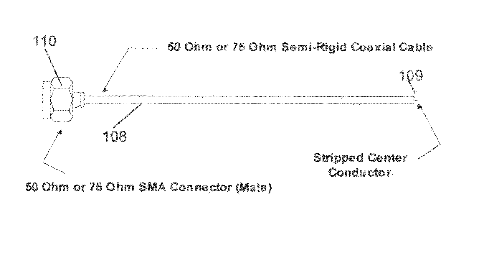
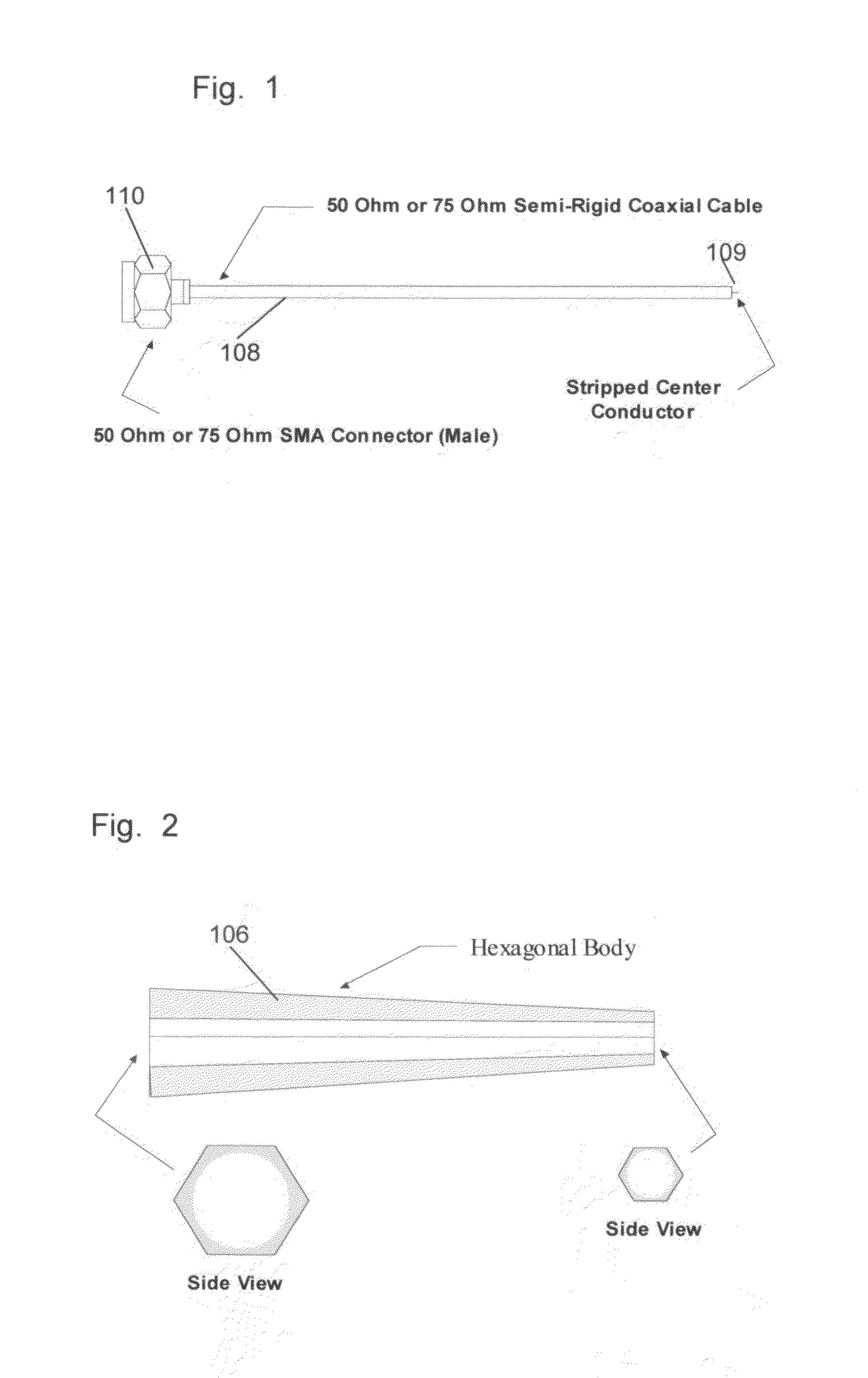
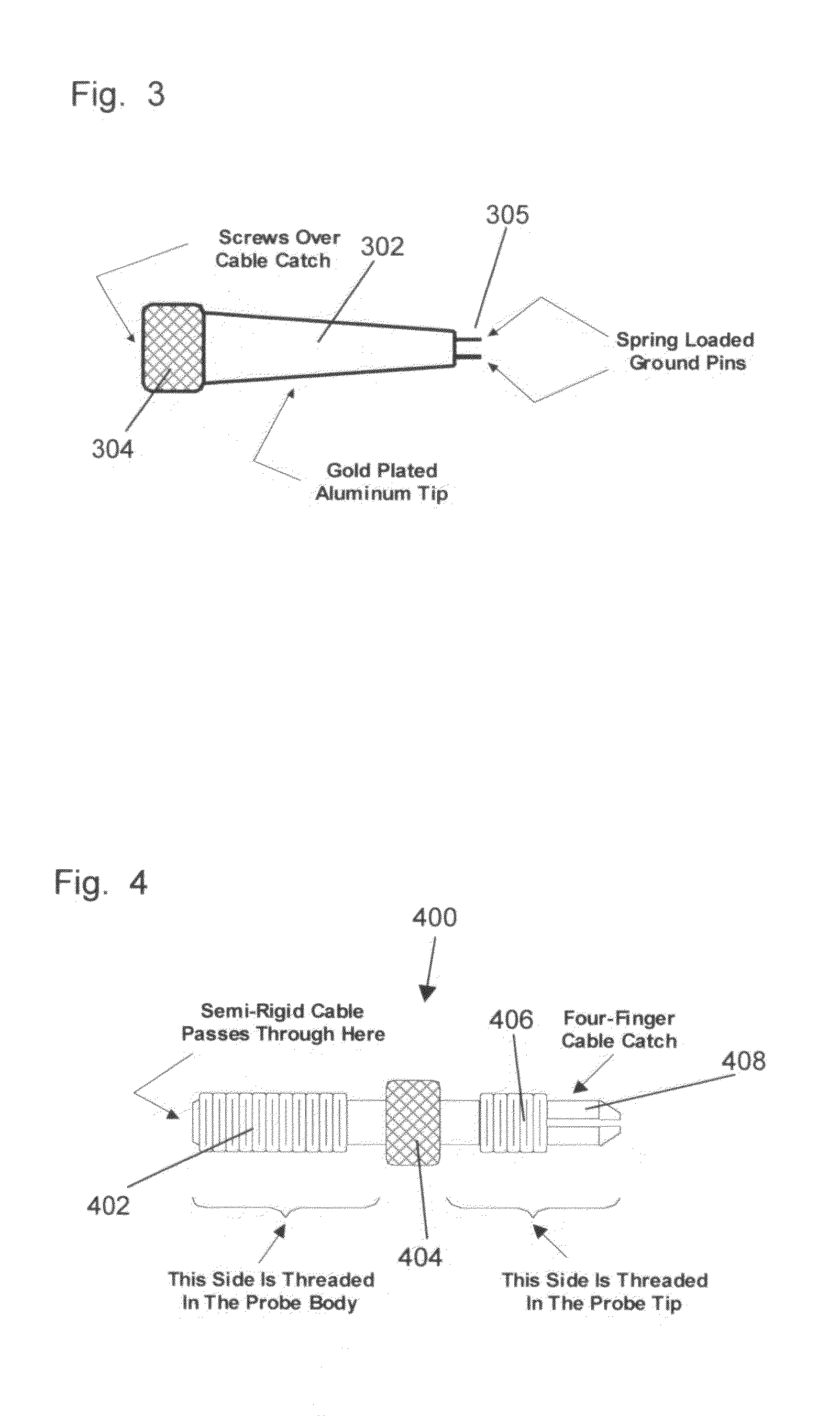
[0007]Briefly, a calibrated high frequency passive impedance probe includes a high-quality low-loss semi-rigid coaxial cable assembly filled with a dielectric material, such as Teflon, and having a silver plated center conductor and silver plated ground outer conductor (jacket) having an SMA male connector on one end and stripped center conductor at the opposite end, and having uniform characteristic impedance along the cable length; a hexagonal shaped body made of black anodized alumin

Problems solved by technology

High frequency impedance measurement systems are typically very expensive and range in the tens of thousand of dollars.
The calibration process often involves a laborious and time consuming process of soldering and de-soldering the cable tip several times to terminate the center conductor into a 50 ohm or 75 ohm load, short and open circuits.
These connectors, which are relatively expensive especially in small quantities, must be soldered to the printed circuit boards.
If the boards are damaged or circuits need to be redesigned which is often the case during prototype stage, RF connectors cannot often be salvaged and after several soldering cycles, removing, and mounting again to multiple printed circuit boards they are rendered useless, or no longer reliable for future use.
Once RF connectors such as SMAs are soldered to a circuit board, they can easily be damaged when they are removed from the circuit board by overheating the solder joints.

Method used


Image

  • Calibrated wideband high frequency passive impedance probe
  • Calibrated wideband high frequency passive impedance probe
  • Calibrated wideband high frequency passive impedance probe

Examples


Embodiment Construction

[0028]Reference herein to “one embodiment”, “an embodiment”, or similar formulations, means that a particular feature, structure, operation, or characteristic described in connection with the embodiment, is included in at least one embodiment of the present invention. Thus, the appearances of such phrases or formulations herein are not necessarily all referring to the same embodiment. Furthermore, various particular features, structures, operations, or characteristics may be combined in any suitable manner in one or more embodiments.

[0029]Generally, an apparatus is provided that is suitable for the purpose of test, characterization, and measurement of electronic components and circuits. More particularly, a calibrated high frequency wide bandwidth passive probe, which is simple to produce and assemble is provided. A passive does not include active components and so power is not required to be provided to a probe in accordance with the present invention.

[0030]Embodiments of the prese...


PUM


Abstract

A calibrated passive impedance probe has a wide bandwidth operating range for impedance and performance measurements of RF and microwave components, devices, and circuits in 50Ω and 75Ω environments. The probe is calibrated at the probe tip, thus allowing accurate impedance and performance measurements of in-circuit functions and on-board components. The calibrated probe can be used to eliminate RF connectors and provide input and output connections to a circuit board for prototype design and quick performance verification thus realizing cost savings on RF connectors. The probe includes a semi-rigid coaxial cable assembly filled with dielectric material, a silver plated center conductor, and silver plated ground outer conductor having an SMA male connector on one end and exposed center conductor at the opposite end and having uniform characteristic impedance of 50Ω or 75Ω along the cable length; a hexagonal shaped body made of anodized aluminum having raised texture on the surface for sure handling; a probe tip of gold plated aluminum with two spring loaded ground pins; a four-finger threaded cable catch for locking semi-rigid coaxial cable assembly inside the tip and for ground continuity from cable to spring loaded pins; an interface RF connector-adapter including SMA female-SMA female, BNC-SMA female, or Type N-SMA female; a locking nut to hold and lock cable assembly and connector-adapter inside the probe body; and 50Ω and 75Ω precision loads for probe calibration.

Description

FIELD OF INVENTION[0001]The present invention relates generally to the field of electronic test and measurement, and more particularly relates to an assembly for a 50 Ohm passive probe.BACKGROUND[0002]It is well-known that measurement, characterization, and testing of electronic circuits are necessary aspects of developing, debugging, and manufacturing electronic products. Typically a test probe is used to make electrical contact with one or more terminals of an electronic circuit, and provide an electrical pathway between that electronic circuit and externally deployed Measurement, characterization, and / or testing equipment. For products that operate at high speeds, it is also known that the impedance of the test probe becomes an important parameter.[0003]It is highly desirable to measure the effective value of passive components (e.g., chip capacitors, inductors, resistors) both at specific frequencies and over specific frequency bands for which those components are being consider...

Claims


Application Information

Patent Timeline
IPC IPC(8): G01R35/00G01R1/067
CPCG01R35/005G01R1/06772
Inventor GHADAKSAZ, MICHAEL M.
Owner AESTECH
Learn More