Method for forming gate oxide of semiconductor device

a gate oxide and semiconductor technology, applied in the direction of semiconductor devices, electrical appliances, basic electric elements, etc., can solve the problems of reducing the yield of patterning process, increasing manufacturing cost and time, and difficulty in securing a margin for patterning process using photoresist, so as to improve the level and threshold voltage of the interface trap charge (dit) and improve the characteristics of gate oxide. , the effect of improving the reliability of the semiconductor devi

Active Publication Date: 2011-03-10
SK KEYFOUNDRY INC
View PDF11 Cites 7 Cited by
  • Summary
  • Abstract
  • Description
  • Claims
  • Application Information

AI Technical Summary

Benefits of technology

[0016]Accordingly, the present invention has been made in view of the above-mentioned problems occurring in the prior art, and it is a primary object of the present invention to provide a method for forming a gate oxide of a semiconductor device, which forms a gate oxide having a triple structure of a wet oxide film / TEOS oxide film / plasma nitride film in a high voltage region of a high voltage element having a triple gate region and hardens the TOES oxide film of the high voltage region according to a high temperature when an oxide film is formed on a medium voltage region to improve uniformity of the TEOS oxide film and enhance electrical characteristic such as threshold voltage characteristic.
[0018]The present invention can form a gate oxide having a triple structure of a wet oxide film / TEOS oxide film / nitride film in a high voltage region and harden the TEOS oxide film when a gate oxide of a medium voltage region is formed to improve characteristics and uniformity of the gate oxide.
[0019]Furthermore, the present invention can form a TEOS oxide film according to an operating voltage to improve an interface trap charge (Dit) level and threshold voltage characteristic so as to enhance the reliability of a semiconductor device employing the TEOS oxide film.

Problems solved by technology

This increases the manufacturing cost and time and decreases production yield.
Furthermore, it is difficult to secure a margin for a patterning process using photoresist as the integration of the semiconductor device increases.
Moreover, a cleaning process is required to selectively remove the oxide films to cause generation of a large number of particles on the surface of the semiconductor substrate.
Furthermore, in the case of the TEOS oxide film formed in the high voltage region A, dangling bonds or other point defects at the TEOS interface are not cured even though thermal budget is applied thereto, and thus a gate leakage current increases.

Method used


Image

  • Method for forming gate oxide of semiconductor device
  • Method for forming gate oxide of semiconductor device
  • Method for forming gate oxide of semiconductor device

Examples


Embodiment Construction

[0024]FIGS. 2a through 2h are cross-sectional views illustrating a method for forming a gate oxide of a semiconductor device according to an embodiment of the present invention.

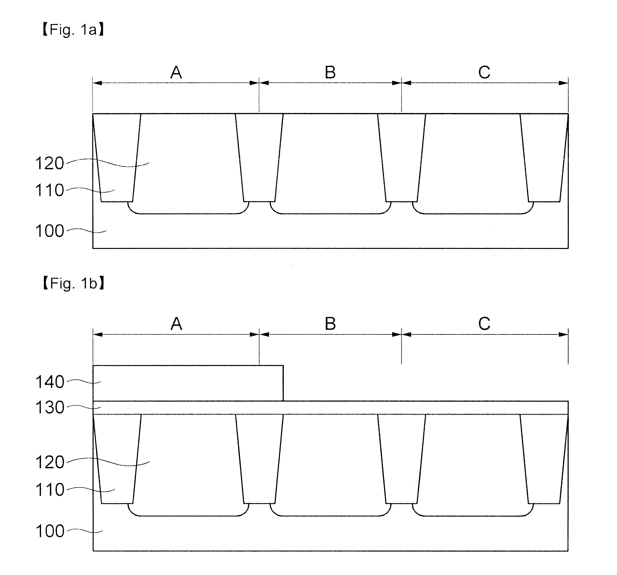
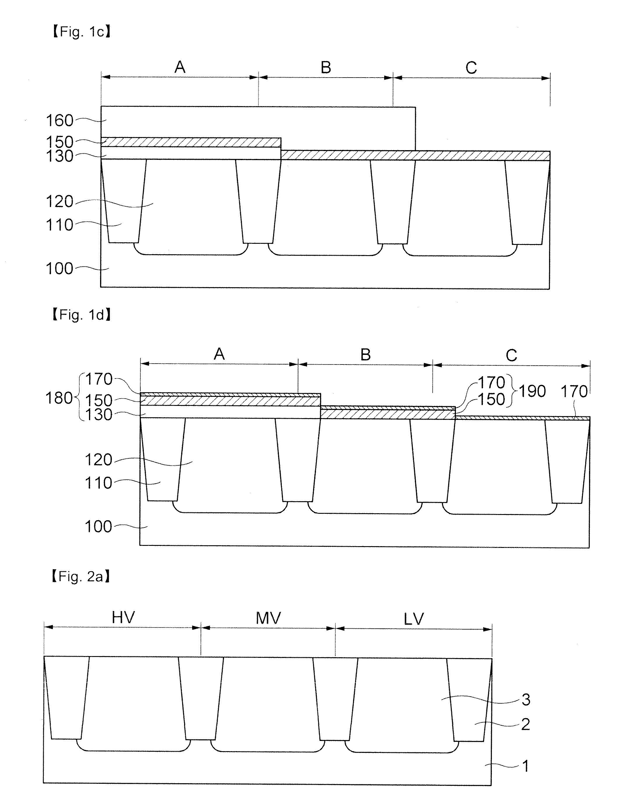
[0025]Referring to FIG. 2a, an isolation layer 2 is formed in a semiconductor substrate 1 to define a high voltage region HV, a medium voltage region MV and a low voltage region LV. Ion implantation is performed to respectively form wells 3 in the high voltage region HV, the medium voltage region MV and the low voltage region LV.

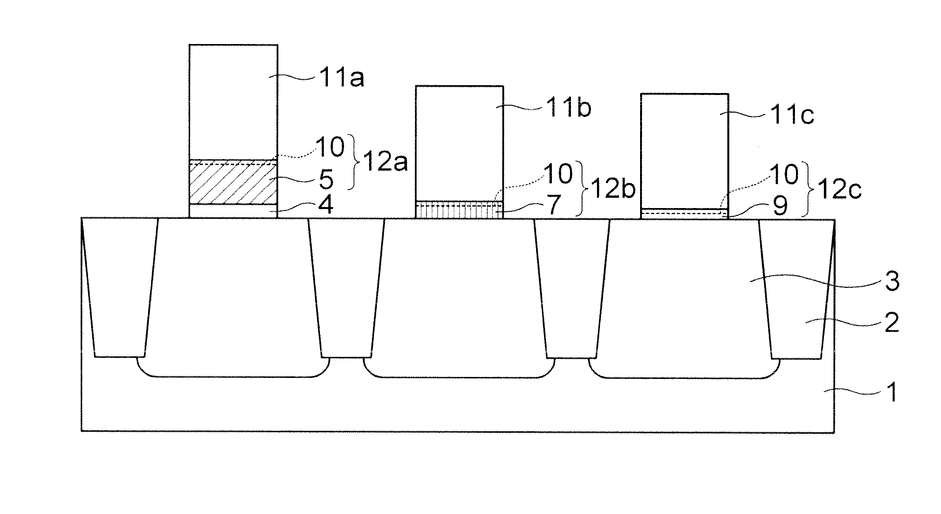
[0026]Referring to FIG. 2b, a first oxide film 4 is formed by a predetermined thickness on the overall surface of the semiconductor substrate 1 and a second oxide film 5 is formed thereon. Here, the first oxide film 4 is formed in order to improve interface trap charge (Dit) characteristic of Si / SiO2 interface.

[0027]The first oxide film 4 is formed of a wet oxide in the ambient of H2 / O2 by a thickness in the range of 40 to 220 Å at a temperature in the range of 800 to 900° C. and the ...


PUM


Abstract

Disclosed herein is a method for forming a triple gate oxide of a semiconductor device. The method for forming a triple gate oxide of a semiconductor device includes the steps of defining a first region where a gate oxide having a first thickness will be formed, a second region where a gate oxide having a second thickness will be formed and a third region where a gate oxide having a third thickness will be formed on a semiconductor substrate, forming a first oxide film through wet oxidation on the semiconductor substrate and forming a second oxide film on the first oxide film, blocking the first region and selectively removing portions the second oxide film and the first oxide film, which are formed on the second region and the third region, forming a third oxide film through thermal oxidation on the semiconductor substrate, blocking the first region and the second region and selectively removing a portion of the third oxide film, which is formed on the third region, and forming a fourth oxide film through thermal oxidation on the semiconductor substrate and then forming a nitride film thereon, wherein a gate oxide having a triple structure of the first oxide film / second oxide film / nitride film is formed in the first region, a gate oxide having a double structure of the third oxide film / nitride film is formed in the second region and a gate oxide having a double structure of the fourth oxide film / nitride film is formed in the third region.

Description

BACKGROUND OF THE INVENTION[0001]1. Field of the Invention[0002]The present invention relates to a method for forming a gate oxide of a semiconductor device, and more particularly, to a method for forming a gate oxide of a semiconductor device with a triple gate oxide having multiple thicknesses.[0003]2. Background of the Related Art[0004]Although conventional semiconductor memory devices have used a gate oxide film having a single thickness, system IC logic products use a semiconductor device having various operating voltages by using gate oxides having multiple thicknesses.[0005]That is, the semiconductor device employs a triple gate oxide structure which includes a thick gate oxide formed in a high voltage region, a thin gate oxide formed in a low voltage region and a gate oxide thinner than the gate oxide formed in the high voltage region, thicker than the gate oxide formed in the lower voltage region and formed in a medium voltage region to achieve appropriate insulation.[0006]...

Claims


Application Information

Patent Timeline
Patent Type & Authority Applications(United States)
IPC IPC(8): H01L29/51
CPCH01L21/28211H01L29/78H01L21/823462H01L21/18
Inventor PARK, JUNG GOO
Owner SK KEYFOUNDRY INC
Why Eureka
Try Eureka