
Solid state storage system with improved data merging efficiency and control method thereof

a storage system and data merging technology, applied in the direction of unauthorized memory use protection, memory adressing/allocation/relocation, instruments, etc., can solve the problems of unable to correctly write predetermined data into a page having such a physical defect, physical defects can also be caused, and the large number of flash memory cells manufactured

Active Publication Date: 2011-03-03
SK HYNIX INC
View PDF6 Cites 18 Cited by
  • Summary
  • Abstract
  • Description
  • Claims
  • Application Information

AI Technical Summary

Benefits of technology

[0011]Embodiments of the present invention provide a control method of controlling a solid state storage system to merge data. In one embodiment of the present invention, a solid state storage system includes: a memory area including a plurality of memory block, and a memory controller configured to regard a first physical block in which a failure is occurred as a temporary block, wherein the first physical block has a first data which was programmed before the failure is occurred and the first data includes a first logical page address, wherein the memory controller is configured to program a second data into a second physical block, as a new physical block and the second data includes a second logical page address in succession to the first logical page address.
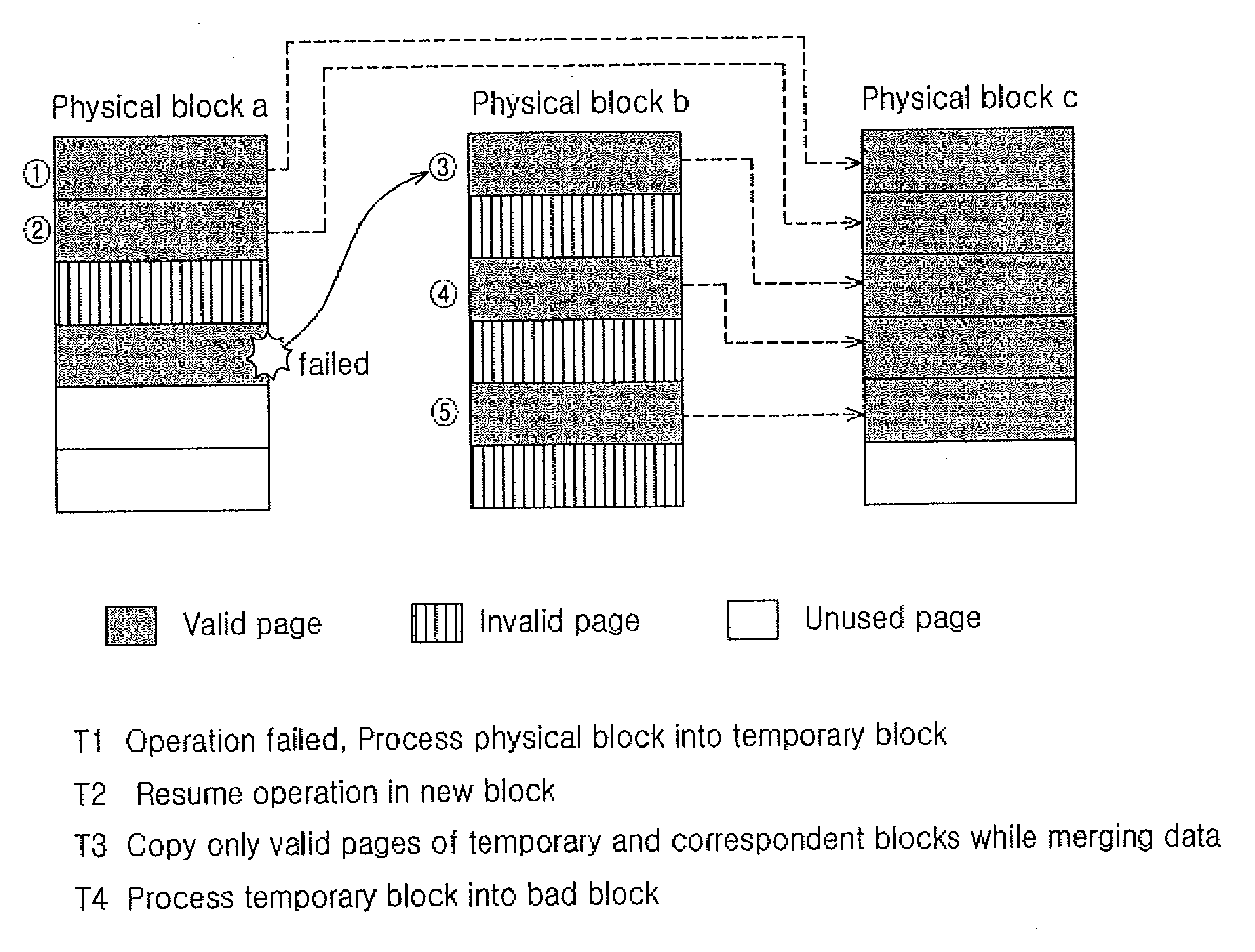
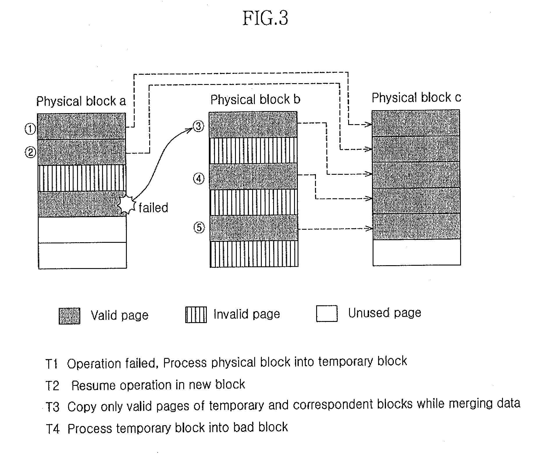
[0012]In another embodiment of the present invention, a solid state storage system includes: a flash memory area configured to include a plurality of memory blocks; a buffer configured to store address mapping and location information of the memory block; and a memory controller configured to control a bad block of the memory blocks and a new physical block, which is associated with the bad block, to link together by a logical address so as to provide an virtual logical block and configured to control information of the link to be stored in the buffer. In yet another embodiment a control method is envisioned of a solid state storage system, such that the method comprises: performing operations on a flash memory area including a plurality of memory blocks; storing address mapping and location information of the memory blocks in a buffer; storing link information of a prior valid page into the buffer wherein the prior valid page is that page in the first bad block which was successfully operated on immediately prior to the failure in the first bad page; allocating a first physical block to resume operations of the bad block past the first bad page by copying all remaining portions of the bad block past the first bad page into the first physical block; updating and storing mapping information of logical and physical addresses in the buffer as a first link index such that the first link index is associated with the remaining portions of the bad block past the first bad page which are copied in the first physical block; and merging together only those valid pages from among the bad block into a final physica

Problems solved by technology

Since semiconductor fabrication processes are carried out in microscopic dimensions, defects can occur when manufacturing the large numbers of flash memory cells.
In addition, physical defects can also be caused by gradual degradation processes that arise from the myriad of write operations that occur because write operations usually require high voltages to be applied at memory cells.
For those and other reasons, it would be impossible to correctly write predetermined data into a page having such a physical defect.
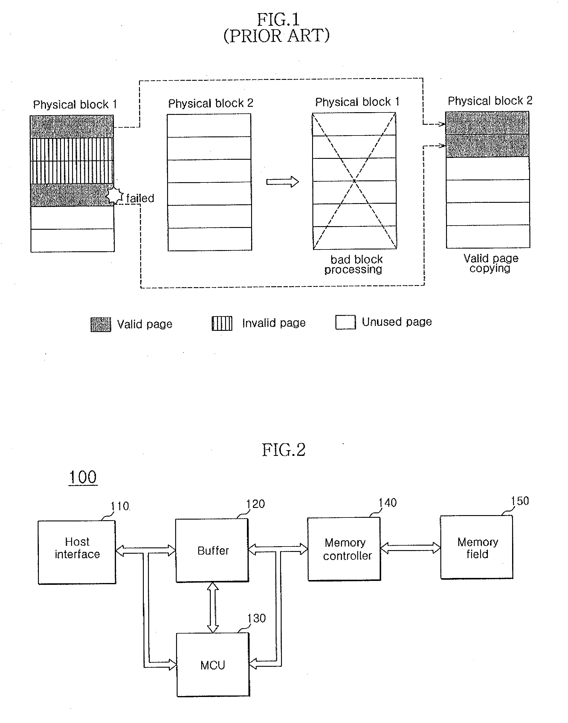
These copying operations are carried out in units of pages and as a result lengthens the data processing time.

Method used


Image

  • Solid state storage system with improved data merging efficiency and control method thereof
  • Solid state storage system with improved data merging efficiency and control method thereof
  • Solid state storage system with improved data merging efficiency and control method thereof

Examples


Embodiment Construction

[0020]Hereinafter, a semiconductor memory apparatus and a test method thereof, according to the present invention, will be described below with reference to the accompanying drawings through exemplary embodiments.

[0021]A solid state storage system according to an embodiment of the present invention will be explained in conjunction with FIG. 2.

[0022]FIG. 2 illustrates a block organization of the solid state storage system embodied in the present invention. Here, the solid state storage system 100 of FIG. 2 is exemplarily reduced in a storage system employing NAND flash memories.

[0023]Referring to FIG. 2, the solid state storage system 100 may comprise a host interface 110, a buffer 120, a micro-control unit (MCU) 130, a memory controller 140 and a memory area 150.

[0024]The host interface 110 is coupled to the buffer 120. The host interface 110 enables an external host (not shown) and the buffer 120 to transmit and receive control commands, address signals and data signals between eac...


PUM


Abstract

The presented solid state storage system provides an efficient manner of processing read and write operations in a memory block that has a faulty page of memory within it. The solid state storage system includes a flash memory area and a memory controller. The memory controller stores link information into a buffer, allocates a first temporary physical block to resume operations of the bad block past the first bad page, updates and stores mapping information associated with the remaining portions of the bad block past the first bad page, and merges together those valid pages from among the bad block into a final physical block by merging together all prior successfully operated valid pages from among the bad block with any subsequently successfully operated valid pages which are associated with successful operations subsequently to the failure in the first bad page of the bad block.

Description

CROSS-REFERENCES TO RELATED APPLICATION[0001]The present application claims priority to Korean application number 10-2009-0082993, filed on Sep. 3, 2009, which is incorporated by reference in its entirety as set forth in full.BACKGROUND[0002]1. Technical Field[0003]Embodiments of the present invention relate generally to a solid state storage system and its control method, and more particularly, to a solid state storage system and a control method thereof.[0004]2. Related Art[0005]Nonvolatile memories are widely employed as storage units in portable information apparatuses. In recent years, there have been proposed solid state drives or disks (SSDs) using NAND flash memories instead of hard disk drives (HDDs) in personal computers, rapidly encroaching the market of HDDs.[0006]Such types of a solid state drives (hereinafter, referred to as “solid state storage system”) are likely to employ flash memories that include a plurality of memory areas in which each memory area is composed o...

Claims


Application Information

Patent Timeline
IPC IPC(8): G06F11/20
CPCG06F11/141G06F11/1666G06F2212/7204G06F12/0246G06F11/20G06F12/06G06F12/14
Inventor KIM, YOUNG HOKIM, KYEONG RHOLEE, MYUNG SUK
Owner SK HYNIX INC
Learn More