Electronic parts packaging structure and method of manufacturing the same
a technology of electronic parts and packaging structure, which is applied in the field of electronic parts packaging structure, can solve the problems of reducing the reliability of connection and easy warping of the semiconductor device, and achieve the effect of increasing the mounting density
- Summary
- Abstract
- Description
- Claims
- Application Information
AI Technical Summary
Benefits of technology
Problems solved by technology
Method used
Image
Examples
first embodiment
[0038](First Embodiment)
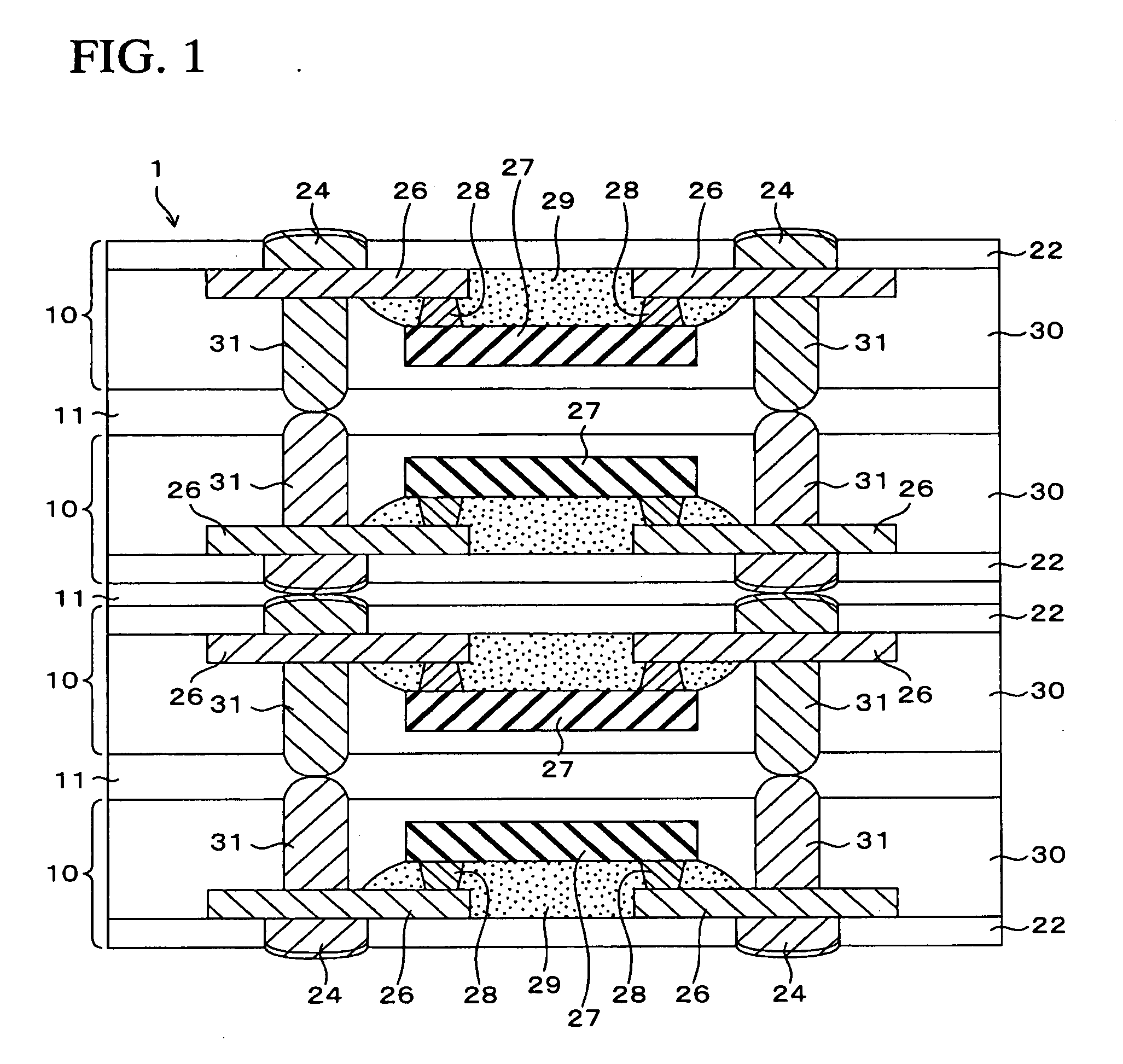
[0039]FIG. 1 is a sectional view showing an electronic parts packaging structure according to a first embodiment of the present invention.
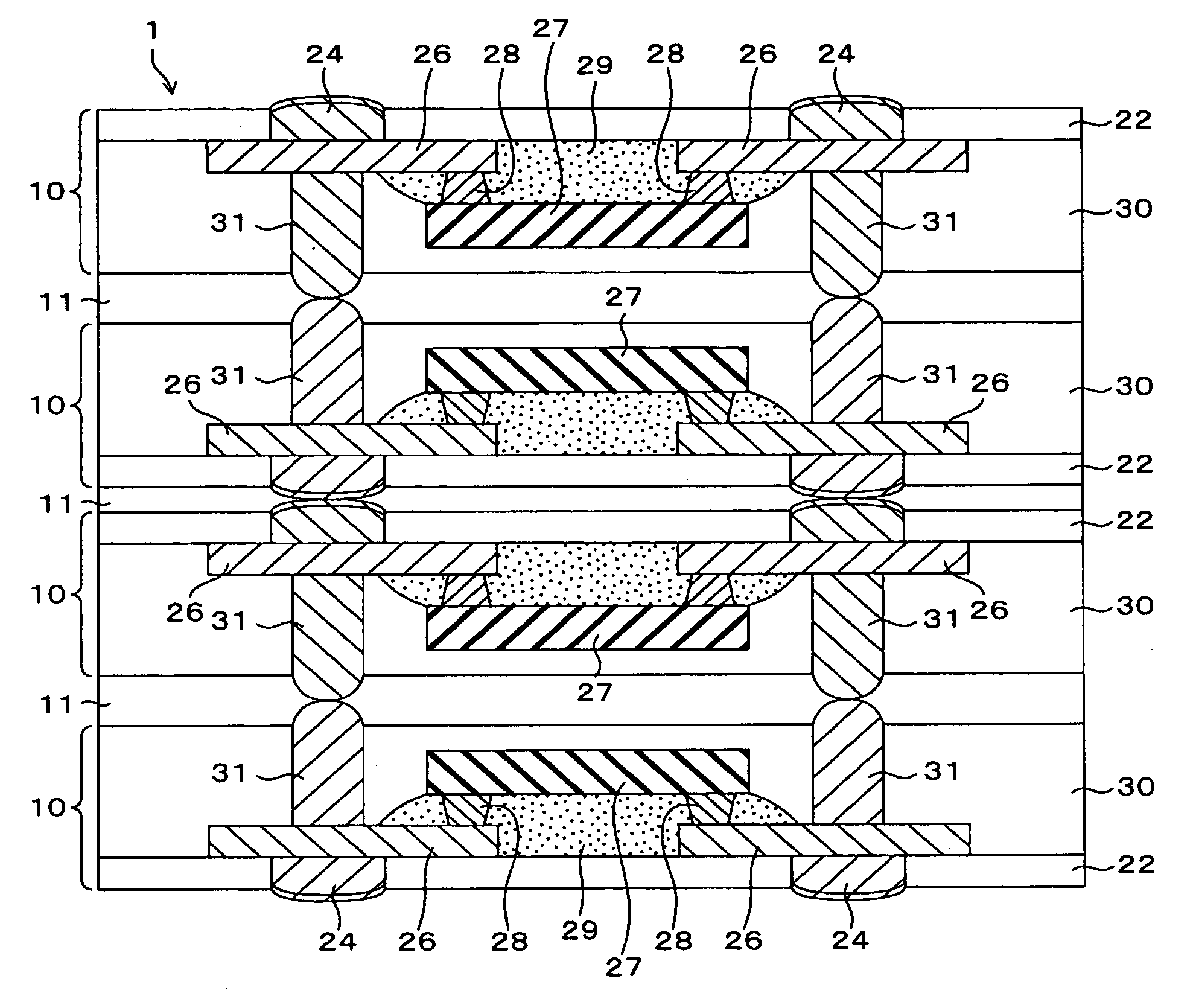
[0040]An electronic parts packaging structure (semiconductor device) 1 of the present embodiment has a structure that plural (four in FIG. 1) sheet(thin film)-like units 10 are stacked to put an insulating layer 11 between them. Each unit 10 is constructed by a insulating resin layer (second insulating layer) 30, a semiconductor chip (electronic parts) 27 buried in the insulating resin layer 30, a solder resist layer (first insulating layer) 22, wirings 26, terminals 24, and contact vias 31. A thickness of one unit 10 is almost 200 μm (almost 100 to 300 μm), for example, and neighboring units 10 in the vertical direction (thickness direction) are electrically connected mutually via the terminals 24 or the contact vias 31 (connecting portions).
[0041]The electronic parts packaging structure 1 of the present embodiment has one...
second embodiment
[0071](Second Embodiment)
[0072]FIG. 4 is a sectional view showing a method of manufacturing an electronic parts packaging structure according to a second embodiment of the present invention, and FIG. 5 is a schematic plan view (general view) showing the same. In FIG. 4, the same reference symbols are affixed to the same constituent parts in FIG. 2N.
[0073]A difference of the present embodiment from the first embodiment is that an edge portion is left like a frame when the substrate 21 is removed by the etching. Since other configurations are basically similar to the first embodiment, explanation of redundant portions will be omitted herein.
[0074]In the first embodiment, in step shown in FIG. 2N, the substrate 21 is removed completely from the unit 10. As described above, since a plurality of units 10 are formed at the same time while using a sheet of substrate 21 in the first embodiment, it may be considered that, depending on the number of the Wilts 10 formed simultaneously, the uni...
third embodiment
[0077](Third Embodiment)
[0078]FIGS. 6A and 6B are sectional views showing a method of manufacturing an electronic parts packaging structure according to a third embodiment of the present invention.
[0079]A difference of the present embodiment from the first embodiment is that the solder resist layer 22 is also formed on the back surface (surface opposite to the semiconductor chip mounting surface) of the substrate 21. Since other configurations are basically similar to the first embodiment, explanation of redundant portions will be omitted herein.
[0080]In the present embodiment, as shown in FIG. 6A, the solder resist layer 22 is formed on both surfaces of the substrate 21. Then, like the first embodiment, as shown in FIG. 6B, the terminals 24 and the wirings 26 are formed and the semiconductor chip 27 is mounted on the wirings 26. Then, the underfill 29 is filled between the semiconductor chip 27 and the wirings 26 and the solder resist layer 22, then the insulating resin layer 30 fo...
PUM
 Abstract
Description
Claims
Application Information
 - R&D
- Intellectual Property
- Life Sciences
- Materials
- Tech Scout
- Unparalleled Data Quality
- Higher Quality Content
- 60% Fewer Hallucinations
Browse by: Latest US Patents, China's latest patents, Technical Efficacy Thesaurus, Application Domain, Technology Topic, Popular Technical Reports.
© 2025 PatSnap. All rights reserved.Legal|Privacy policy|Modern Slavery Act Transparency Statement|Sitemap|About US| Contact US: help@patsnap.com


