Pulsed deposition and recrystallization and tandem solar cell design utilizing crystallized/amorphous material

Inactive Publication Date: 2011-02-17
VARIAN SEMICON EQUIP ASSOC INC
View PDF20 Cites 11 Cited by
  • Summary
  • Abstract
  • Description
  • Claims
  • Application Information

AI Technical Summary

Problems solved by technology

Higher temperature tolerant glass panels such as quartz or sapphire panel exist; however, the high cost of such glasses discourages their use.
The low temperature deposition process, however, does not yield optimal silicon film.
Although ELA and SLS processes may result in a panel with mono-crystalline or poly-crystalline silicon thin film, each process is not without disadvantages.
For example, excimer lasers used in both processes may be expensive to operate, resulting in an expensive TFT.
In addition, the duty cycle may not be optimum for the best conversion of amorphous silicon into crystalline silicon.
Further, the excimer laser may have pulse-to-pulse variations and spatial non-uniformity in the delivered power that may affect the uniformity of the processes.
There may also be intra-pulse non-uniformity that may be caused by for example, self-interference of the beam.
Such inter-pulse and intra-pulse non-uniformity may result in silicon films with non-uniform crystals.
These issues also exist in the manufacturing of solar cells.

Method used


Image

  • Pulsed deposition and recrystallization and tandem solar cell design utilizing crystallized/amorphous material
  • Pulsed deposition and recrystallization and tandem solar cell design utilizing crystallized/amorphous material
  • Pulsed deposition and recrystallization and tandem solar cell design utilizing crystallized/amorphous material

Examples


Embodiment Construction

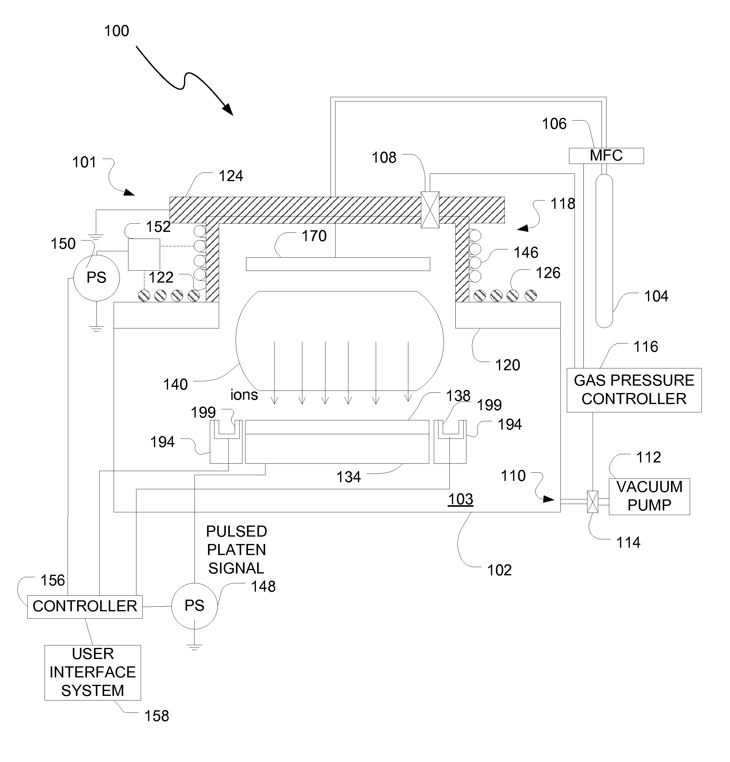
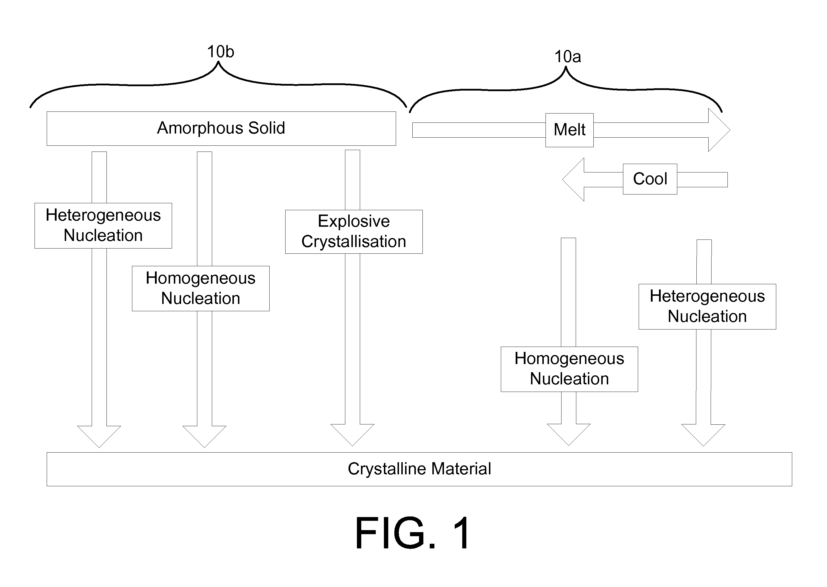
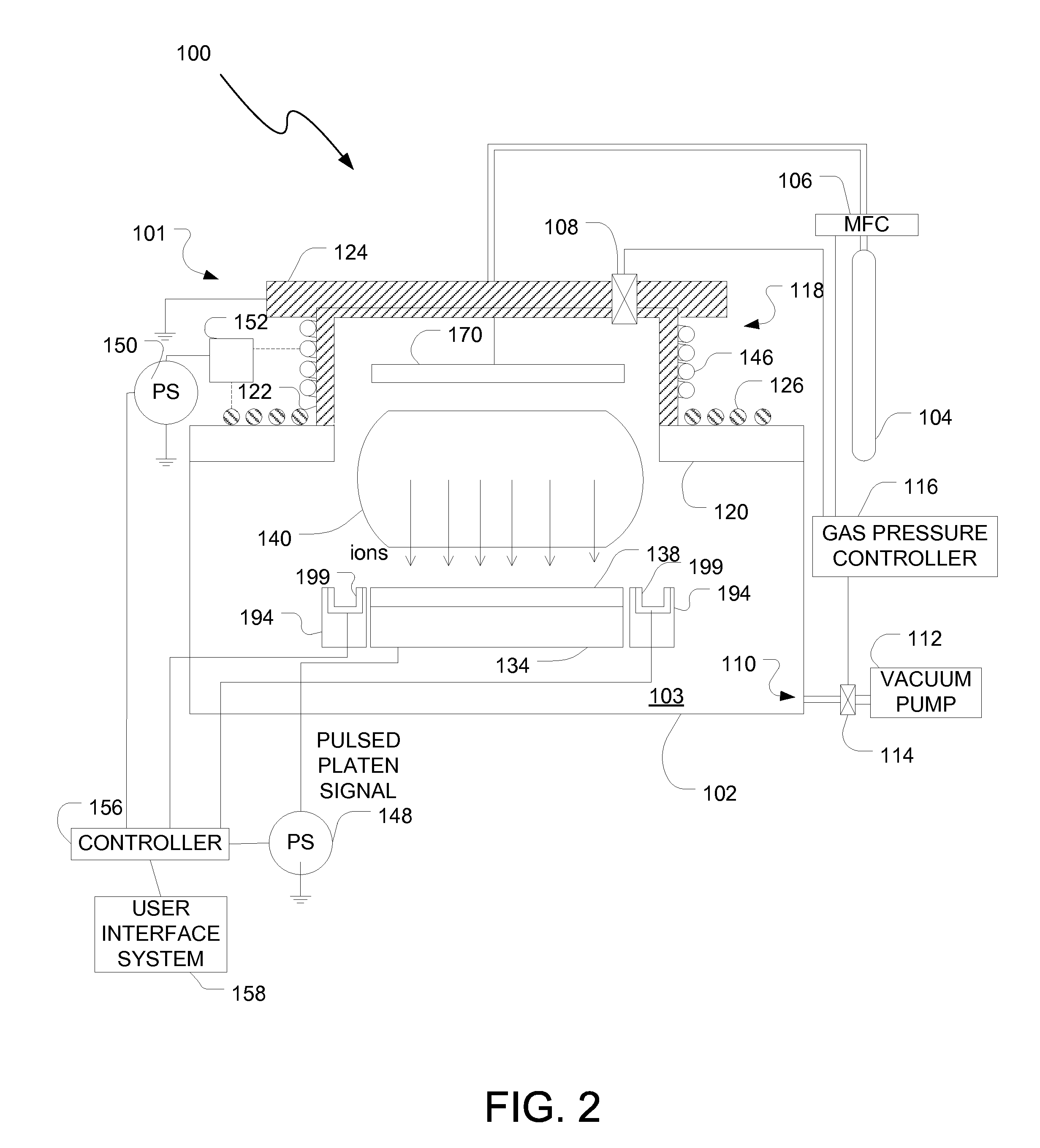
[0017]As described above, high temperature annealing, such as by use of laser, can be expensive, thereby making it an unattractive alternative for the creation of FPDs and solar cells. Thus, alternative methods of creating crystalline silicon are desired.

[0018]In the present disclosure, several embodiments are described using a substrate. This substrate may be a wafer (for example, a silicon wafer) or a substrate comprising a plurality of films. In addition, the substrate may be an elemental substrate containing only one element (e.g. silicon wafer or metal foil); a compound substrate containing more than one element (e.g. SiGe, SiC, InTe, GaAs, InP, GaInAs, GaInP; CdTe; CdS; and combinations of (Cu, Ag and / or Au) with (Al, Ga, and / or In) and (S, Se and / or Te) such as CuInGaSe, CuInSe2, other group III-V semiconductors and other group II-VI compounds); and / or an alloy substrate. The material contained in the substrate may be metal, semiconductor, and / or insulator (e.g. glass, Polyet...


PUM

PropertyMeasurementUnit
Pressureaaaaaaaaaa
Flow rateaaaaaaaaaa
Electric potential / voltageaaaaaaaaaa

Abstract

A method of depositing and crystallizing materials on a substrate is disclosed. In a particular embodiment, the method may include creating a plasma having deposition-related species and energy-carrying species. During a first time period, no bias voltage is applied to the substrate, and species are deposited on the substrate via plasma deposition. During a second time period, a voltage is applied to the substrate, which attracts ions to and into the deposited species, thereby causing the deposited layer to crystallize. This process can be repeated until an adequate thickness is achieved. In another embodiment, the bias voltage or bias pulse duration can be varied to change the amount of crystallization that occurs. In another embodiment, a dopant may be used to dope the deposited layers.

Description

BACKGROUND OF THE INVENTION[0001]The widespread adoption of emerging technologies such as flat panel displays (FPD) and solar cells depends on the ability to manufacture electrical devices on low cost substrates. In manufacturing FPD, pixels of a typical low cost flat panel display (FPD), are switched by thin film transistors (TFT) which may be typically manufactured on thin (−50 nm thick) films of amorphous silicon deposited on inert, glass substrates. However, improved FPDs demand better performing pixel TFTs, and it may be advantageous to manufacture high performance control electronics directly onto the panel. One advantage may be to eliminate the need for costly and potentially unreliable connections between the panel and external control circuitry.[0002]Current FPDs contain a layer of silicon that is deposited onto the glass panel of the display via a low temperature deposition process such as sputtering, evaporation, plasma enhanced chemical vapor deposition (PECVD), or low p...

Claims


Application Information

Patent Timeline
IPC IPC(8): C23C14/14C23C14/00
CPCH01L21/0237H01L21/02381H01L21/0245H01L21/02505H01L21/0251H01L21/02532Y02E10/546H01L21/02667H01L21/2236H01L31/0725H01L31/182H01L31/1872H01L21/0259Y02P70/50H01L21/02H01L31/04
Inventor MAYNARD, HELENPAPASOULIOTIS, GEORGE D.SINGH, VIKRAMHATEM, CHRISTOPHERGODET, LUDOVIC
Owner VARIAN SEMICON EQUIP ASSOC INC
Why Eureka
Try Eureka