Insulated Gate Bipolar Transistor (IGBT) Collector Formed with Ge/A1 and Production Method

a technology of ion implantation and collector, which is applied in the direction of semiconductor devices, electrical equipment, transistors, etc., can solve the problems of high cost of ion implantation equipment and complicated process control, higher device voltage drop when the igbt is turned, and undesirable increase of the igbt turn-off time, so as to reduce the production cost and improve the device parameter performance of the igbt produ

Inactive Publication Date: 2010-12-30
ALPHA & OMEGA SEMICON INC
View PDF5 Cites 13 Cited by
  • Summary
  • Abstract
  • Description
  • Claims
  • Application Information

AI Technical Summary

Benefits of technology

[0006]An object of the present invention is to provide an IGBT collector formed with Ge / Al thin films and its fabrication method that is applicable to both non punch through and punch through IGBTs. The method should effectively reduce production cost and improve device parameter performance of the IGBT product.

Problems solved by technology

As a result, this requires expensive ion implantation equipment and complicated process control.
However, due to the use of Al as P-type impurity in this method, it brings about two problems.
One problem is that contact resistance is high, which consequently leads to higher device voltage drop when the IGBT is turned on.
Another problem is that the higher injection efficiency of cavity leads to an undesirable increase of IGBT turn-off time.
In summary, existing structures and production methods of IGBTs use ion implantation machine to implant P-type dopants into back surface of silicon substrate to form IGBT collector and this incurs high cost.

Method used


Image

  • Insulated Gate Bipolar Transistor (IGBT) Collector Formed with Ge/A1 and Production Method
  • Insulated Gate Bipolar Transistor (IGBT) Collector Formed with Ge/A1 and Production Method
  • Insulated Gate Bipolar Transistor (IGBT) Collector Formed with Ge/A1 and Production Method

Examples


Embodiment Construction

[0038]The description above and below plus the drawings contained herein merely focus on one or more currently preferred embodiments of the present invention and also describe some exemplary optional features and / or alternative embodiments. The description and drawings are presented for the purpose of illustration and, as such, are not limitations of the present invention. Thus, those of ordinary skill in the art would readily recognize variations, modifications, and alternatives. Such variations, modifications and alternatives should be understood to be also within the scope of the present invention.

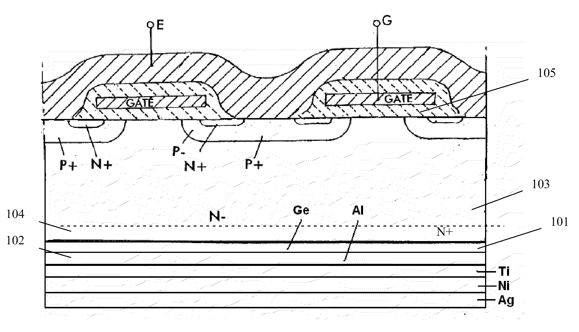
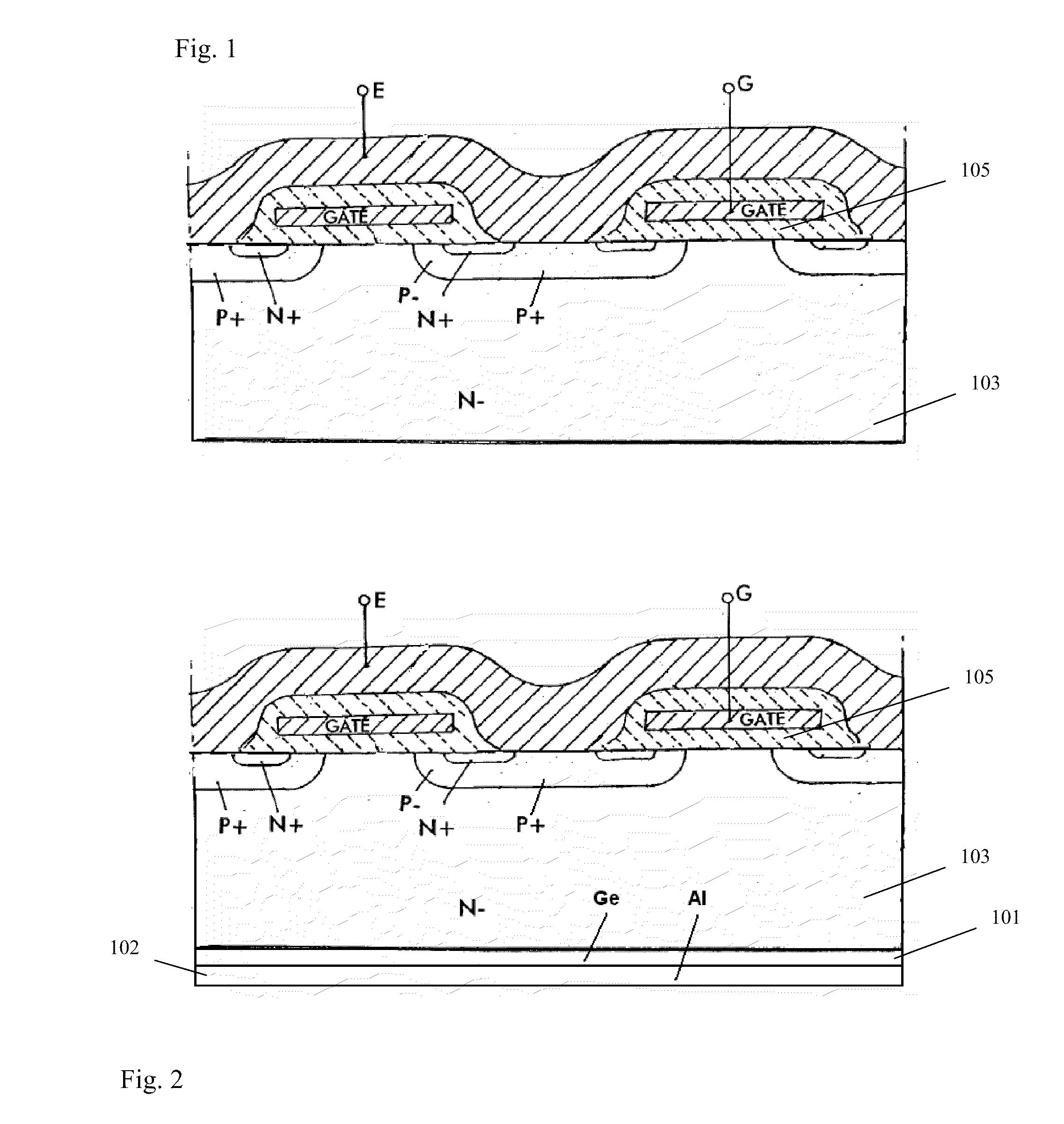
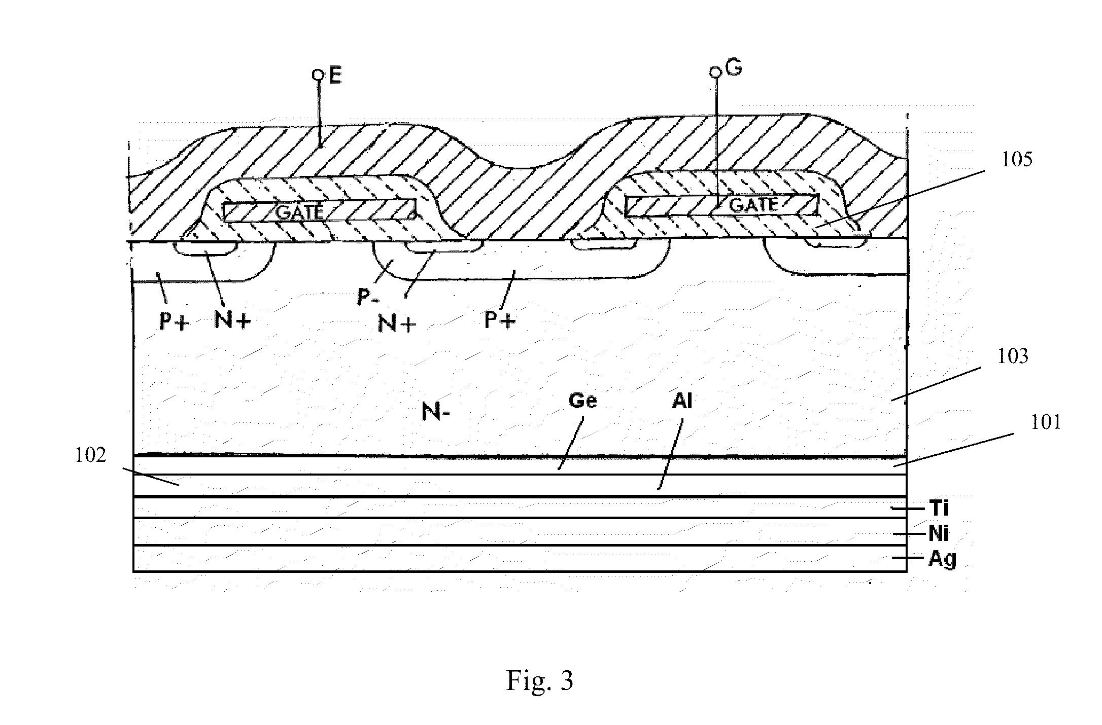
[0039]As illustrated in FIG. 2, the structure of a non punch through IGBT is formed on the top of an N− type Si substrate layer 103(drift region). There is an N+ type source region of high dopant density disposed on a top surface of the Si substrate and surrounded by a P-channel region. A P+ type source electrode shorting region of high dopant density is provided to improve the body-sou...


PUM

PropertyMeasurementUnit
temperatureaaaaaaaaaa

Abstract

This invention discloses an IGBT device with its collector formed with Ge/Al and associated method of fabrication. The collector is formed on the substrate layer, which is on the back of IGBT, and contains Ge and Al thin films. After thinning and etching the back side of IGBT substrate, Ge and Al are sequentially deposited to form Ge/Al thin films on the back surface of the substrate. An annealing process is then carried out to diffuse Al into Ge thin film layer to form a P-doped Ge layer functioning as the IGBT collector. The present invention is applicable to both non punch through IGBTs as well as punch through IGBTs.

Description

CROSS REFERENCE TO RELATED APPLICATIONSField of Invention[0001]This invention relates generally to the field of semiconductor electronics. More specifically, the present invention is directed to the structural design and fabrication of a semiconductor device.BACKGROUND OF THE INVENTION[0002]During an insulated gate bipolar transistor (IGBT) manufacturing process a collector is formed on the back side of silicon substrate. Currently both non punch through type and punch through type IGBTs utilize back side ion implantation method to implant dopants, of opposite conductivity type to the substrate dopants, onto a silicon substrate back surface to counter dope the substrate and then heat anneal it to activate the implanted dopants thus forming a collector. As a result, this requires expensive ion implantation equipment and complicated process control.[0003]For instance, U.S. Pat. No. 7,005,702 discloses a non punch through type IGBT with transparent amorphous silicon collector or anode ...

Claims


Application Information

Patent Timeline
Patent Type & Authority Applications(United States)
IPC IPC(8): H01L29/739H01L21/20
CPCH01L29/0834H01L29/7395H01L29/66333H01L29/165
Inventor HUANG, PINGFENG, TAOWU, RUISHENGCHEN, YIDUAN, LEI
Owner ALPHA & OMEGA SEMICON INC
Why Eureka
Try Eureka