
Method for providing solder connection, electronic equipment and method for manufacturing same

a technology of electronic equipment and solder connection, which is applied in the direction of manufacturing tools, sustainable manufacturing/processing, and final product manufacturing, etc., can solve problems such as electrical coupling failure, and achieve the effects of stable junction shape, enhanced electrical coupling, and high efficiency

Inactive Publication Date: 2010-12-16
SUMITOMO BAKELITE CO LTD
View PDF4 Cites 9 Cited by
  • Summary
  • Abstract
  • Description
  • Claims
  • Application Information

AI Technical Summary

Benefits of technology

The present invention provides a method for improving the reliability of solder connections in electronic equipment. The method involves using an adhesive agent layer with a flux function to enhance the electrical coupling between solder bumps and protruded electrodes. The adhesive agent layer is formed by heating and compressing the solder bump and protruded electrode while they are in mutual facing arrangement. The method allows for the elimination of residue in the contact point of the solder bump and protruded electrode, resulting in enhanced electrical coupling. The invention also provides an electronic equipment with improved reliability.

Problems solved by technology

However, in the technology described in Patent Document 1, the binding material coated with a metalized pattern is caught between the solder bump and the metalized pattern, causing a problem of an electrical coupling failure.

Method used


Image

  • Method for providing solder connection, electronic equipment and method for manufacturing same
  • Method for providing solder connection, electronic equipment and method for manufacturing same
  • Method for providing solder connection, electronic equipment and method for manufacturing same

Examples


example 7

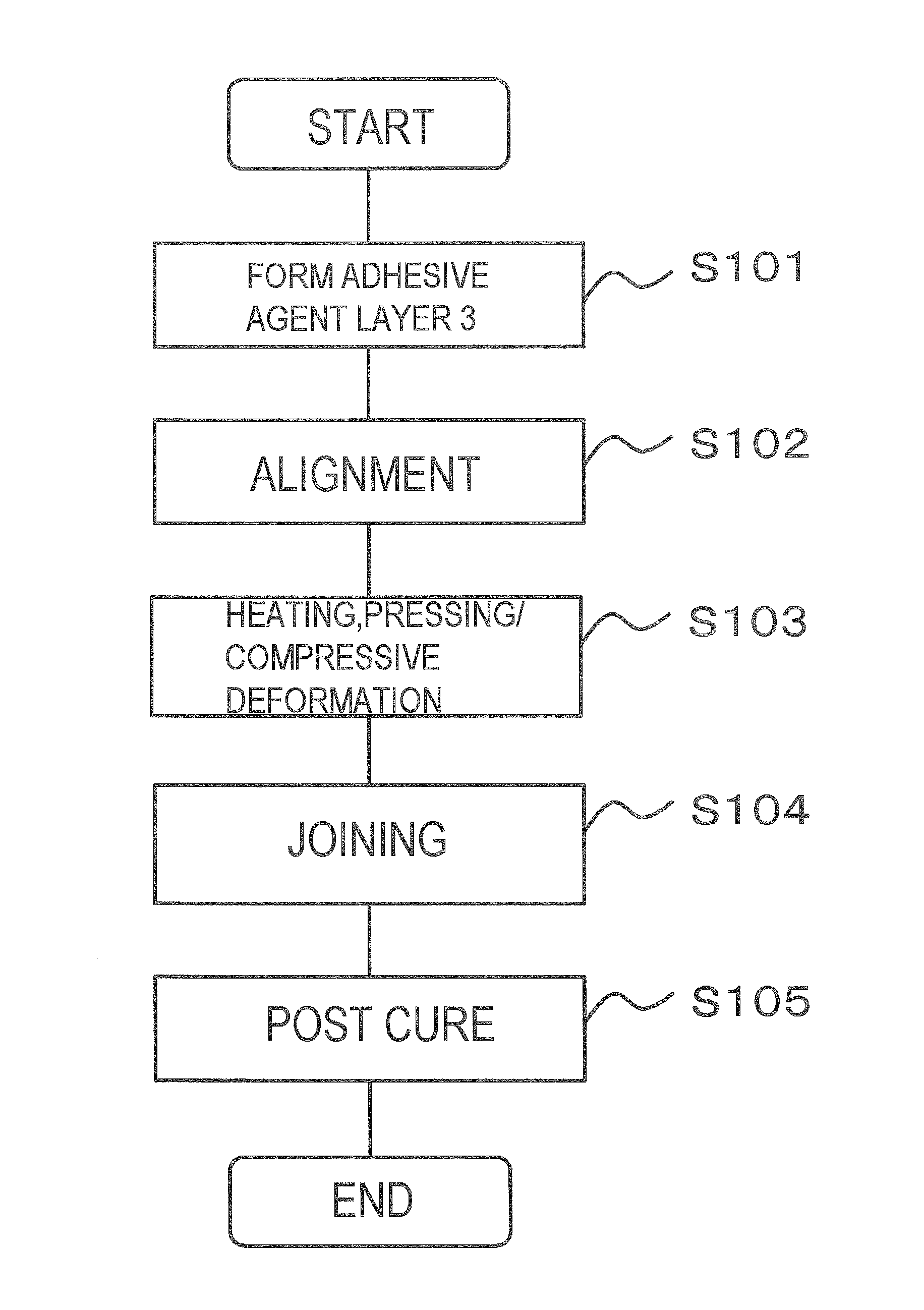
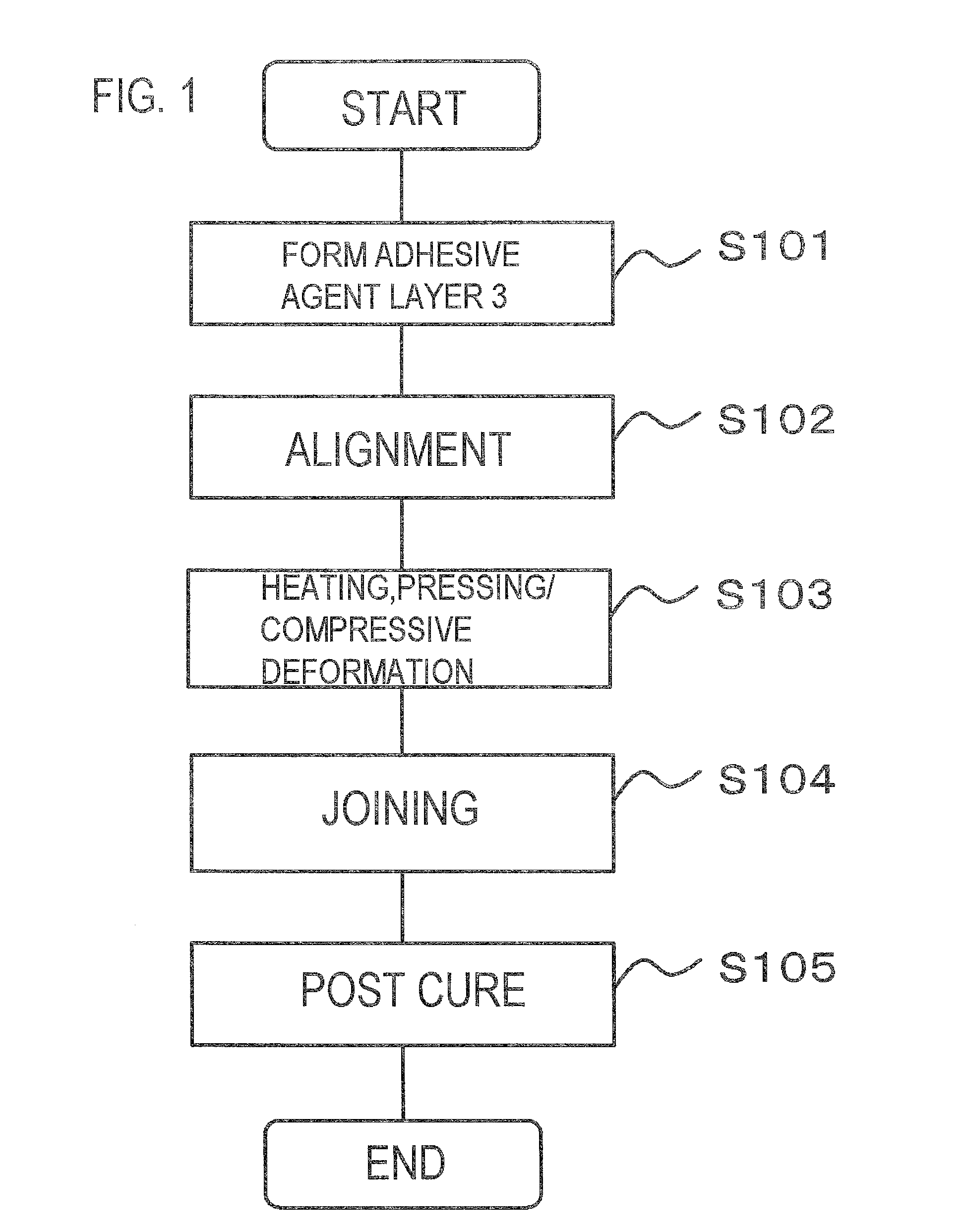
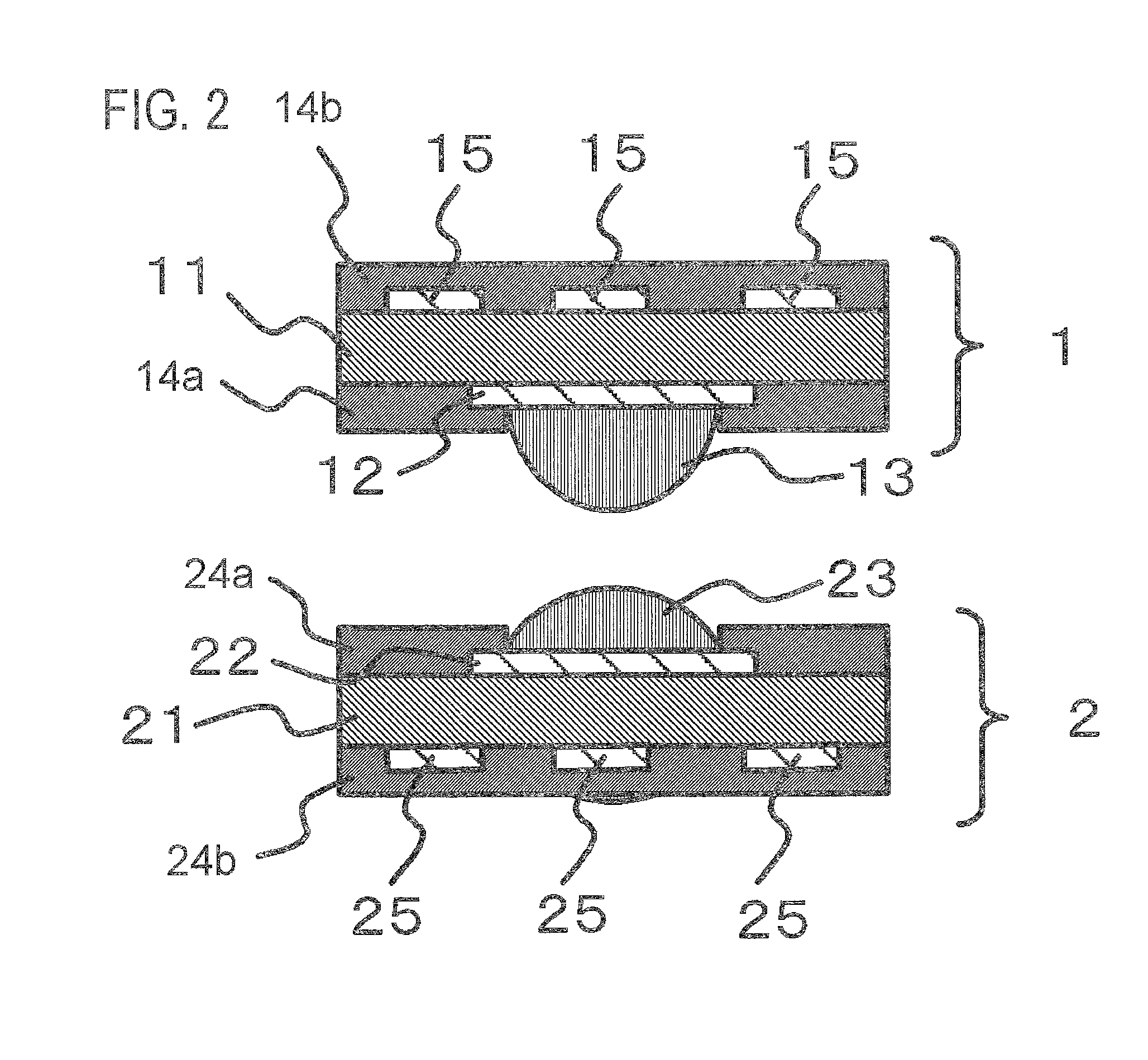
[0124]According to the process for manufacturing the electronic component as described above, the first substrate (substrate with solder bump) having the solder bump of a height above the solder resist of 40 μm and the second substrate (substrate with solder bump) having the solder bump of a height above the solder resist of 40 μm were obtained. Subsequently, as described above, the solder bump of the first substrate is joined to the solder bump of the second substrate by employing the adhesive tape of example 1 to manufacture the multiple-layered circuit board (electronic component). The connectivity, the junction cross section, and the expansion of the adhesive agent layer by the compression were evaluated for the obtained multiple-layered circuit boards according to the above-described method.

[0125]In example 7, [total of height of the solder bumps A+B]-[film thickness C]=50 μm before the compressive deformation, and [total of height of the solder bumps D+E] after the compressive...

example 8

[0126]According to the process for manufacturing the electronic component as described above, the first substrate (substrate with solder bump) having the solder bump of a height above the solder resist of 18 μm and the second substrate (substrate with solder bump) having the solder bump of a height above the solder resist of 18 μm were obtained. Subsequently, as described above, the solder bump of the first substrate is joined to the solder bump of the second substrate by employing the adhesive tape of example 1 to manufacture the multiple-layered circuit board (electronic component). The connectivity, the junction cross section, and the expansion of the adhesive agent layer by the compression were evaluated for the obtained multiple-layered circuit boards according to the above-described method.

[0127]In example 8, [total of height of the solder bumps A+B]-[film thickness C]=6 μm before the compressive deformation, and [total of height of the solder bumps D+E] after the compressive ...


PUM

PropertyMeasurementUnit
melt viscosityaaaaaaaaaa
frequencyaaaaaaaaaa
heightaaaaaaaaaa

Abstract

The method for providing the solder connection of the present invention is a method for providing a solder connection, which electrically connects a first electronic component having a solder bump to a second electronic component having a protruded electrode to provide electrical connection between the first solder bump and the protruded electrode, wherein a relation of: A+B>C is satisfied, where a height of the first solder bump from one surface of the first electronic component is presented as A [μm], a height of the protruded electrode before the compressive deformation from one surface of the second electronic component is presented as B [μm], and a thickness of the adhesive agent layer is presented as C [μm], and further comprising: disposing the adhesive agent layer in the first electronic component; and deforming the first solder bump and the protruded electrode and providing a contact of the above-described protruded electrode with the above-described first solder bump, so that the sum of the height A [μm] of the first the solder bump and the height B [μm] of the above-described protruded electrode is substantially equivalent to the thickness C [μm] of the above-described adhesive agent layer.

Description

TECHNICAL FIELD[0001]The present invention relates to a method for providing a solder connection, an electronic equipment and a method for manufacturing same.BACKGROUND ART[0002]Requirements for enhanced characteristics and lighter and more compact features of electronic equipments in recent years promote high-density integration and high-density installation of electronic components such as semiconductor packages and the like, and miniaturization and high pin count of such electronic components are progressing. A solder joint is employed for obtaining electric coupling for the electronic components, and for example, it is employed for a conducting junction between semiconductor chips, a conducting junction between a semiconductor chip and a circuit board such as such as a package having a flip-chip device installed therein, a conducting junction between a circuit board and a circuit board. Further, requirements for reduced thickness, miniaturization, fine-pitch junction for electro...

Claims


Application Information

Patent Timeline
Patent Type & Authority Applications(United States)
IPC IPC(8): H01R43/16
CPCH01L24/13H01L2924/00014H01L24/73H01L24/81H01L24/92H01L2224/13022H01L2224/81193H01L2224/81204H01L2224/81801H01L2224/83191H01L2224/83855H01L2224/92H01L2924/01004H01L2924/01013H01L2924/01029H01L2924/01033H01L2924/01059H01L2924/01078H01L2924/01079H01L2924/01082H01L2924/01327H05K3/305H05K3/3436H05K3/3489H05K2201/0382H05K2201/10977H05K2203/0485H01L24/29H01L2224/0554H01L2224/73104H01L2924/0105H01L2924/01005H01L2924/01006H01L2924/01047H01L2924/01072H01L2924/014Y10T29/49144Y10T29/49151H01L2924/15787Y10T29/49149Y10T29/49204Y02P70/613H01L2224/05567H01L2224/05573H01L2224/81H01L2224/83H01L2924/3512H01L2924/00H01L2224/05599H01L2224/0555H01L2224/0556Y02P70/50
Inventor MEURA, TORU
Owner SUMITOMO BAKELITE CO LTD
Learn More