Optimized process for fabricating light-emitting devices using artificial materials

a technology of artificial materials and fabrication processes, applied in semiconductor devices, lasers, semiconductor lasers, etc., can solve the problems of complex treatment, inability to obtain suitable refractive index material, and inability to achieve suitable refractive index

Active Publication Date: 2010-11-18
THALES SA
View PDF5 Cites 9 Cited by
  • Summary
  • Abstract
  • Description
  • Claims
  • Application Information

AI Technical Summary

Benefits of technology

[0025]Advantageously, the high-reflectivity structure consists of an alternation of strata comprising etched subwavelength periodical structures enabling the effective refractive index of each of the strata, and consequently that of the high-reflectivity structure, to be fixed.

Problems solved by technology

However, since the number of existing materials is limited, it is very difficult and constricting to obtain a material to be deposited that has the suitable refractive index.
However, another major drawback associated with this technology remains.
Since the size of the chips does not exceed a few millimeters in width for a few millimeters in length, these treatments prove to be complicated.
In addition, as regards QCLs, because of the long emission wavelengths of the latter (these sources are used in ranges that may go from the infrared range to the THz range), the thicknesses of the deposited layers rapidly reach critical values, posing problems such as mechanical integrity or induced strain problems.
Consequently, the uncertain reliability of these complex treatments is currently putting off their use.
However, it is very difficult at the present time to produce lasers using this technology.
Furthermore, the cleaving carried out, to singularize the laser cavities, does not enable their lengths to be guaranteed.
Consequently, the fabrication processes for such lasers is at the present time complex, costly and of uncertain quality.
To summarize, the existing technologies for improving the efficiency of light emitters, such as laser sources for example, notably by means of antireflection treatments, are difficult to implement.
In addition, their performance and their reliability are not guaranteed.

Method used


Image

  • Optimized process for fabricating light-emitting devices using artificial materials
  • Optimized process for fabricating light-emitting devices using artificial materials
  • Optimized process for fabricating light-emitting devices using artificial materials

Examples


Embodiment Construction

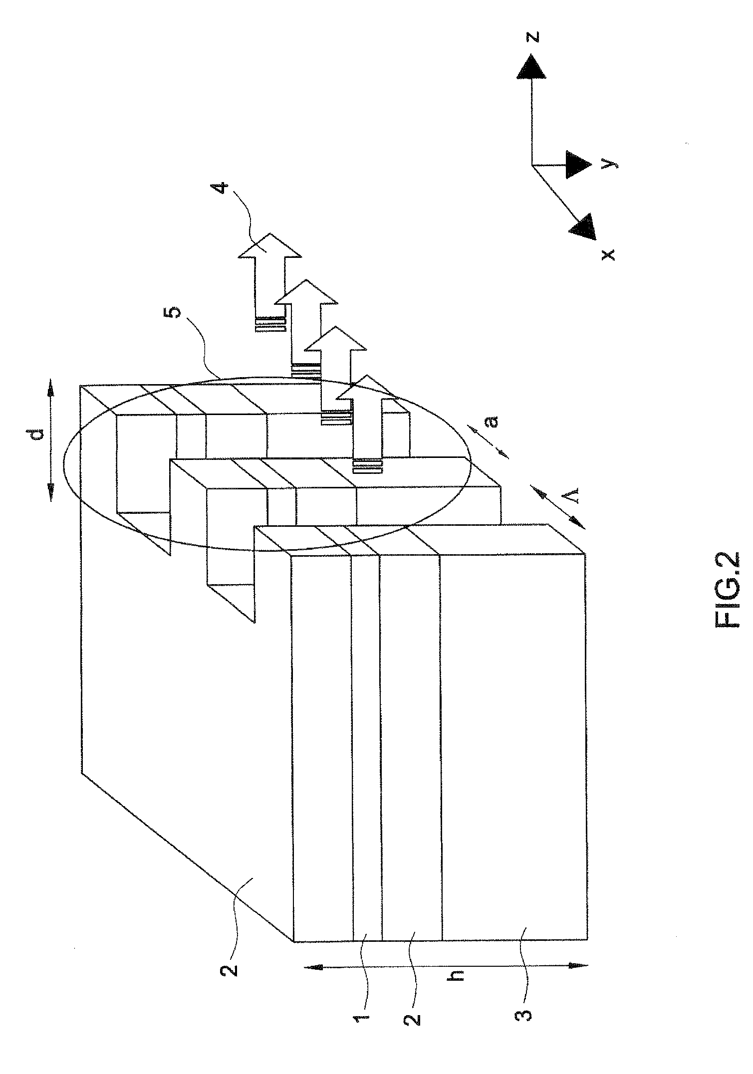
[0041]FIG. 1 shows a simplified diagram of the operation of a quantum cascade laser according to the prior art. The cascade laser differs from conventional lasers by the specificity of its active zone 1. This is formed from a number of periods each consisting of several tens of epitaxially grown layers of semiconductor materials (such as, for example, InGaAs, AlInAs, GaAs, AlGaAs or InP).

[0042]When an electric current is injected into this active zone 1, the electrons acquire energy that they restore by the cascade effect, each time in the form of a photon. The engineering of the material (nature of the semiconductor, thickness of the epitaxially grown layers, etc.) determines the emission wavelength of the laser. The waveguides 2 enable the light output by the laser in the form of a beam 4 to be amplified. Moreover, the active zone 1 and the waveguides 2 are grown on any substrate 3 that provides the function of a mechanical support.

[0043]In general, the reflection loss at the outp...


PUM


Abstract

The present invention relates to a process for fabricating light-emitting devices. More particularly, the aim of the invention is to allow the fabrication of light emitters with improved efficiency by using artificial materials, enabling antireflection or high-reflectivity treatments to be carried out.For this purpose, subwavelength structures are etched on one of the ends of an emissive cavity, enabling the external face to be controlled.The invention applies to any light emitter, and therefore notably to lasers and more particularly still to QCLs (quantum cascade lasers).Moreover, the fabrication process according to the invention is preferably a wafer-scale process

Description

PRIORITY CLAIM[0001]This application claims priority to PCT Patent Application Number PCT / EP2008 / 057254, entitled Method of Manufacturing Optimized Light Devices Using Artificial Materials, filed Jun. 11, 2008.TECHNICAL FIELD[0002]The present invention relates to a process for fabricating light-emitting devices. More precisely, the aim of the invention is to produce light emitters of improved efficiency by the use of artificial materials, said artificial materials enabling precise antireflection or high-reflectivity treatments to be carried out. Moreover, the fabrication process according to the invention has the advantage of being a wafer-scale process and of reducing the number of technological steps required.[0003]The invention applies to any light emitter or amplifier, and therefore notably to lasers, and more particularly still to QCLs (quantum cascade lasers). The case of cascade lasers will be more particularly explained by an example of the invention.BACKGROUND OF THE INVENT...

Claims


Application Information

Patent Timeline
IPC IPC(8): H01L33/46H01L21/78H01L33/44
CPCB82Y20/00H01L33/10H01L33/20H01L33/22H01S5/3402H01S5/105H01S5/1082H01S5/1096H01S5/125H01S5/028H01S5/11
Inventor LEE-BOUHOURS, MANE-SI LAURE
Owner THALES SA
Why Eureka
Try Eureka