
Making colloidal ternary nanocrystals

a technology of colloidal nanocrystals and nanocrystals, which is applied in the direction of polycrystalline material growth, crystal growth process, after-treatment details, etc., can solve the problems of high cost, low efficiency and increased radiative lifetime of colloidal quantum dots compared with their self-assembled counterparts, etc., to achieve short radiative lifetime, short radiative lifetime, and stable fluorescence

Inactive Publication Date: 2010-11-18
EASTMAN KODAK CO
View PDF3 Cites 93 Cited by
  • Summary
  • Abstract
  • Description
  • Claims
  • Application Information

AI Technical Summary

Benefits of technology

[0026]It is an advantage of the present invention that the colloidal ternary nanocrystals made in accordance with the present method exhibit the desirable properties of single molecule non-blinking (>1 minute), short radiative lifetimes (<10 ns), and stable fluorescence following high temperature anneals. It is an important feature of the invention that the ternary cores have a gradient in alloy composition in order to achieve the non-blinking and short radiative lifetime properties. Another advantage of the present invention is that colloidal ternary core / shell nanocrystals exhibiting these properties can be used to create advantaged quantum dot phosphors, medical and biological sensors, single photon LEDs, and high efficiency LEDs and lasers.
that the colloidal ternary nanocrystals made in accordance with the present method exhibit the desirable properties of single molecule non-blinking (>1 minute), short radiative lifetimes (<10 ns), and stable fluorescence following high temperature anneals. It is an important feature of the invention that the ternary cores have a gradient in alloy composition in order to achieve the non-blinking and short radiative lifetime properties. Another advantage of the present invention is that colloidal ternary core / shell nanocrystals exhibiting these properties can be used to create advantaged quantum dot phosphors, medical and biological sensors, single photon LEDs, and high efficiency LEDs and lasers.

Problems solved by technology

The blinking behavior of quantum dots, however, is generally considered an intrinsic limitation that is difficult to overcome.
The results of Hohng et al and Larson et al do not solve the intrinsic problems resulting in blinking dots, they only control the environment at the surface of the dots in order to mitigate the problem.
In addition to the problem of blinking, colloidal quantum dots suffer from increased radiative lifetimes as compared with their self-assembled counterparts.
Because of problems, such as, aggregation of the quantum dots in the emitter layer, the efficiency of these devices was rather low in comparison with typical OLED devices.
The efficiency was even poorer when a neat film of quantum dots was used as the emitter layer (Hikmet et al., J. Appl. Phys. 93, 3509 (2003)).
The poor efficiency was attributed to the insulating nature of the quantum dot layer.
Regardless of any future improvements in efficiency, these hybrid devices still suffer from all of the drawbacks associated with pure OLED devices.
The resulting device had a poor external quantum efficiency of 0.001 to 0.01%.
These organic ligands are insulators and would result in poor electron and hole injection into the quantum dots.
In addition, the remainder of the structure is costly to manufacture, due to the usage of electron and hole semiconducting layers grown by high vacuum techniques, and the usage of sapphire substrates.
Despite these advantages, quantum dot phosphors have not been introduced into the marketplace due to some major shortcomings; such as, poor temperature stability and insufficient (10-30%) quantum yields for phosphor films with high quantum dot packing densities.
The disadvantage of this approach is that the resulting quantum dot phosphor films are unacceptably thick (1 mm), as compared to the desired thickness of 10 μm.
To date, optoelectronic devices or biological (medical) studies have not had colloidal quantum dots (or nanocrystals) available that are inherently non-blinking or that have short radiative lifetimes. Previous methods to create non-blinking dots are application dependent and not universally applicable across the technical disciplines utilizing quantum dots.

Method used


Image

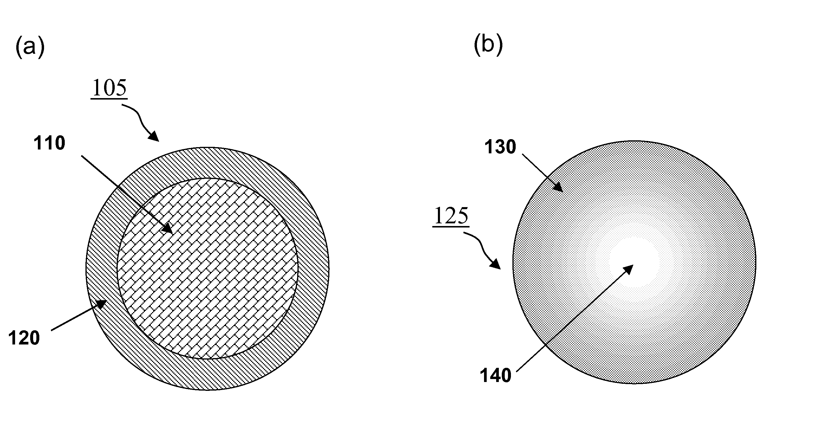
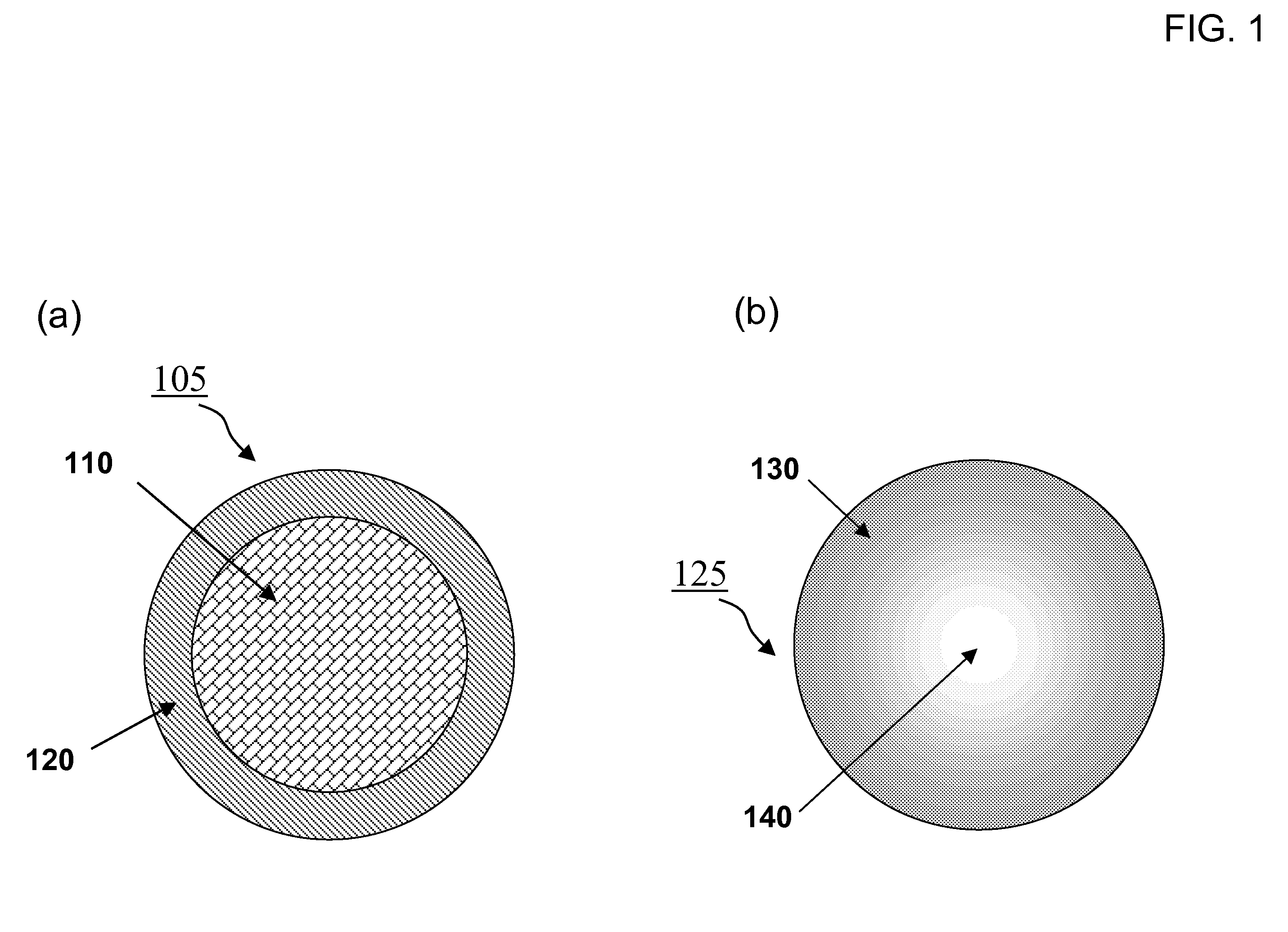
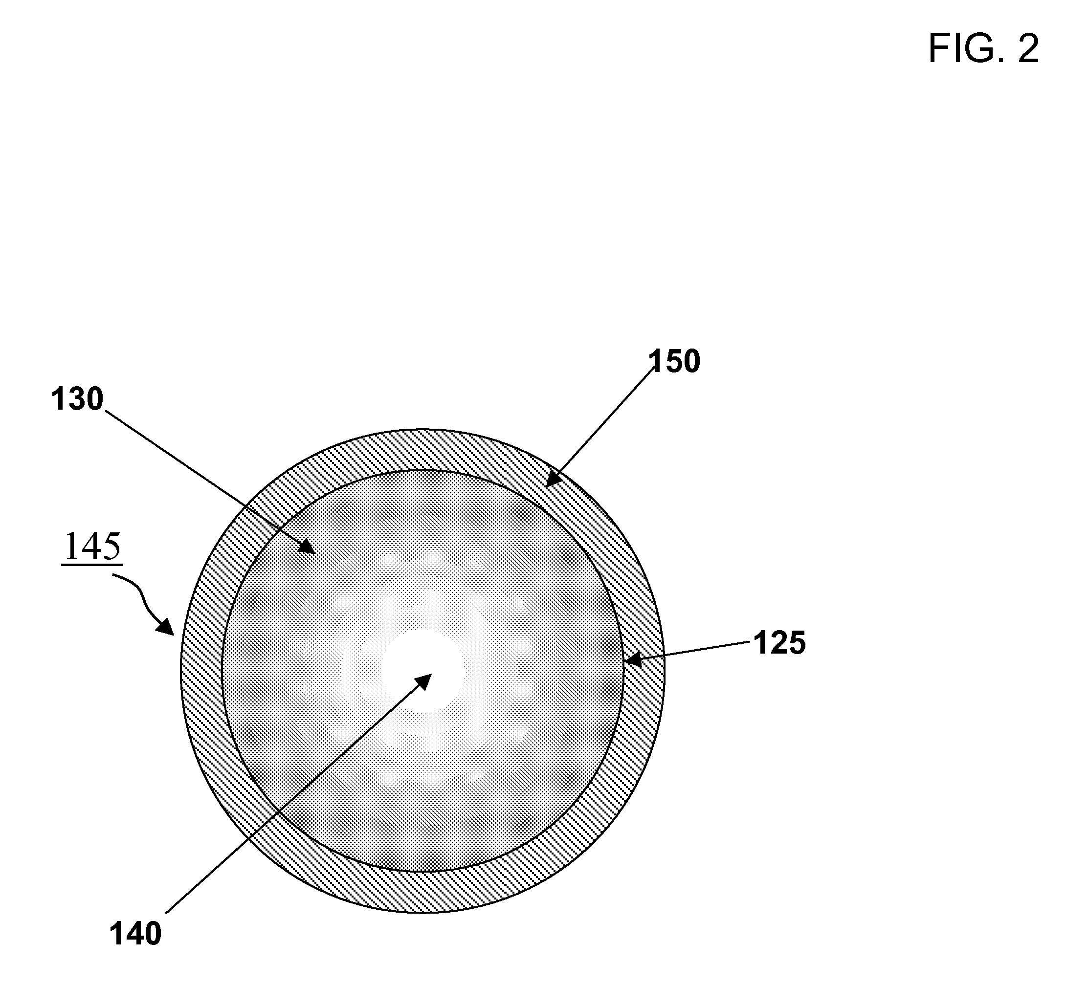
  • Making colloidal ternary nanocrystals
  • Making colloidal ternary nanocrystals
  • Making colloidal ternary nanocrystals

Examples


example i-1

Inventive Example I-1

Preparation of the Inventive Ternary Core / Shell Non-Blinking Nanocrystals, CdxZn1-xSe / ZnSe

[0053]All synthetic routes were carried out using standard airless procedures with a dry box and a Schlenk line. The first step in creating the ternary cores was to form CdSe cores. Typically, 0.0755 g of TDPA (1-tetradecylphosphonic acid), 4 g of pre-degassed TOPO (trioctylphosphine oxide), and 2.5 g of HDA (hexadecylamine) were added in a three-neck flask. The mixture was degassed at 100° C. for half an hour. The stock solution of 1 M TOPSe was prepared by dissolving of 0.01 mol selenium in 10 ml TOP (trioctylphosphine). 1 ml of TOPSe was added to the flask and the mixture was heated to 300° C. The cadmium stock solution (0.06 g of CdAc2 in 3 ml TOP) was quickly injected under vigorous stirring resulting in nucleation of CdSe nanocrystals, after which time the temperature was set at 260° C. for further growth. After 5-10 min, the heating was removed and the flask was allo...

example i-2

Inventive Example I-2

Preparation of the Inventive Ternary Core / Shell Non-Blinking Nanocrystals, CdxZn1-xSe / ZnSeS

[0056]All synthetic routes were carried out using standard airless procedures with a dry box and a Schlenk line. The first step in creating the ternary cores was to form CdSe cores. In a three-neck flask, 0.2 mmol of CdO and 0.5 g of stearic acid were heated to 180° C. until the mixture went clear. Inside of a dry box, 3 ml of HDA and 6 ml of TOPO were added to the mixture. On a Schlenk line the mixture was heated to 310° C. under vigorous stirring, whereupon 1 ml of 1 M TOPSe was injected. The temperature was then lowered to 290-300° C. and stirred for an additional 10 minutes.

[0057]Next a ZnSe shell was formed on the CdSe cores. After cooling the core crude solution back to room temperature, it was reheated to 190° C. In a syringe was added 260 μl of 1M diethylzinc in hexane, 260 μl of 1M TOPSe, and 2 ml of TOP. The contents of the syringe were then added to the CdSe cor...


PUM

PropertyMeasurementUnit
temperatureaaaaaaaaaa
external quantum efficiencyaaaaaaaaaa

Abstract

A method of making a colloidal solution of ternary semiconductor nanocrystals, includes providing binary semiconductor cores; forming first shells on the binary semiconductor cores containing one of the components of the binary semiconductor cores and another component which when combined with the binary semiconductor will form a ternary semiconductor, thereby providing core / shell nanocrystals; and annealing the core / shell nanocrystals to form ternary semiconductor nanocrystals containing a gradient in alloy composition.

Description

CROSS-REFERENCE TO RELATED APPLICATIONS[0001]Reference is made to commonly assigned U.S. patent application Ser. No. 11 / 226,622 filed Sep. 14, 2005, entitled “Quantum Dot Light Emitting Layer” by Keith B. Kahen; U.S. patent application Ser. No. 11 / 683,479 filed Mar. 8, 2007, entitled “Quantum Dot Light Emitting Device” by Keith B. Kahen; and U.S. patent application Ser. No. 11 / 770,8334 filed Jun. 29, 2007, entitled “Light-Emitting Nanocomposite Particles” by Keith B. Kahen, the disclosures of which are incorporated herein.STATEMENT REGARDING FEDERALLY-SPONSORED RESEARCH OR DEVELOPMENT[0002]This invention was made with Government support under Cooperative Agreement #DE-FC26-06NT42864 awarded by DOE. The Government has certain rights in this invention.FIELD OF THE INVENTION[0003]The present invention relates to making colloidal solutions of ternary nanocrystals.BACKGROUND OF THE INVENTION[0004]Colloidal semiconductor nanocrystals, or quantum dots, have been the focus of a lot of resea...

Claims


Application Information

Patent Timeline
Patent Type & Authority Applications(United States)
IPC IPC(8): H01L29/38H01L21/20
CPCC09K11/02C09K11/88C09K11/883C30B7/00C30B33/02C30B29/48C30B29/50C30B29/60C30B29/40
Inventor KAHEN, KEITH B.REN, XIAOFAN
Owner EASTMAN KODAK CO
Learn More