Semiconductor device and method for manufacturing the same

a technology of semiconductors and semiconductors, applied in the direction of semiconductor devices, basic electric elements, electrical equipment, etc., can solve the problems of reducing the dislocation density not always matching, deteriorating breakdown voltage, and difficulty in reducing the dislocation density

Inactive Publication Date: 2010-09-30
FURUKAWA ELECTRIC CO LTD
View PDF3 Cites 30 Cited by
  • Summary
  • Abstract
  • Description
  • Claims
  • Application Information

AI Technical Summary

Problems solved by technology

However, when the crystal is grown by using the MOCVD method or the like, the condition of reducing the dislocation density does not always match with the condition of increasing the carbon concentration.
In fact, when the GaN semiconductor layer is grown by the MOCVD method, there arises a problem that although it is possible to improve the electron mobility by reducing the dislocation density by increasing the growth temperature, the breakdown voltage also deteriorates because the carbon concentration within the crystal decreases in the same time.
In particular, the GaN epitaxially grown on a Si substrate has a problem that it is extremely difficult to reduce the dislocation density while keeping the carbon concentration high because dislocations occur in high concentration due to a large difference of lattice constants of the substrate and the GaN layer and an enough effect cannot be obtained even if the dislocation density is to be reduced by the growth condition.

Method used


Image

  • Semiconductor device and method for manufacturing the same
  • Semiconductor device and method for manufacturing the same
  • Semiconductor device and method for manufacturing the same

Examples


embodiment

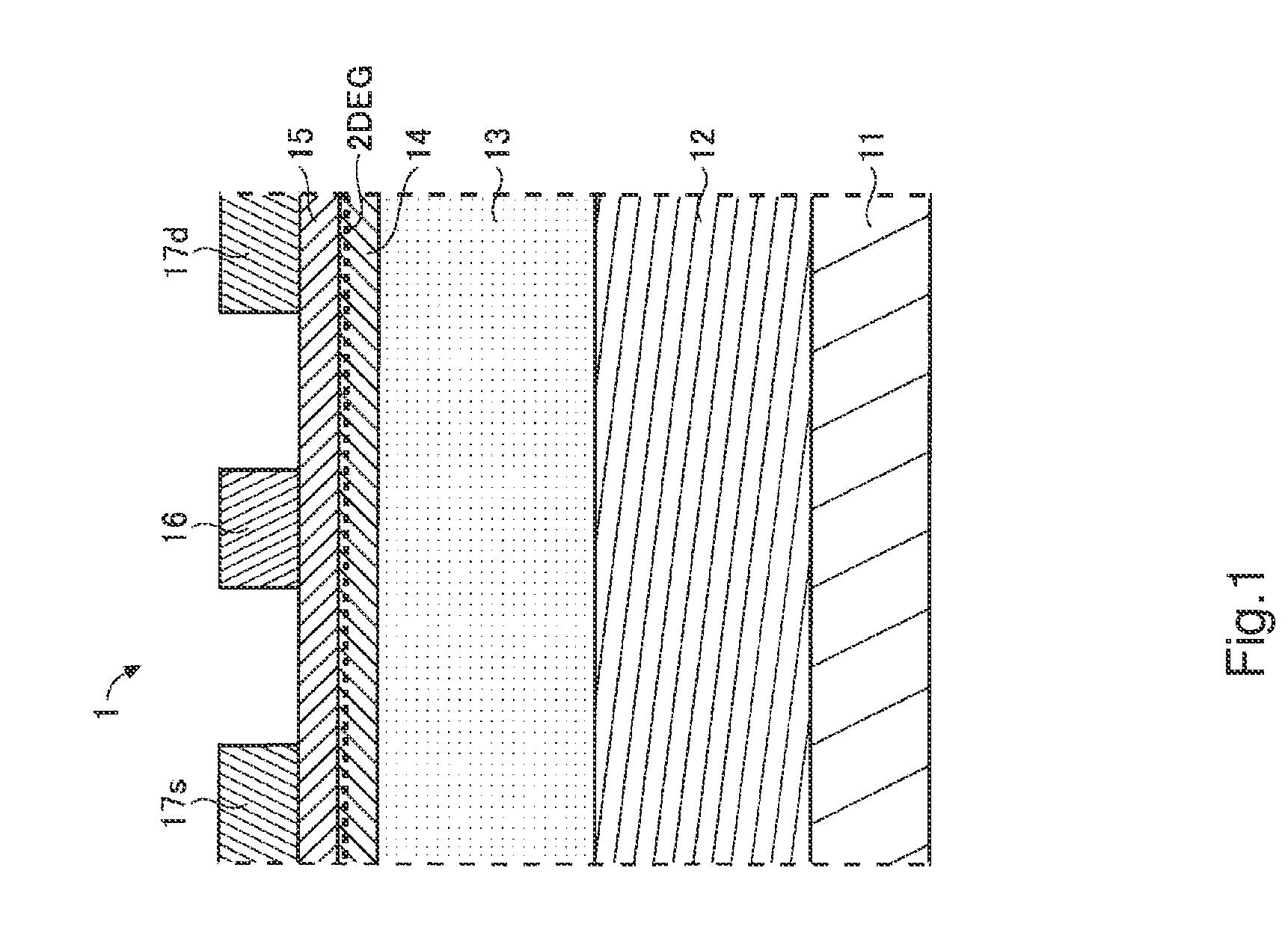
[0021]A method for fabricating a semiconductor device of one embodiment of the invention will now be explained in detail with reference to the drawings. It is noted that the invention is not limited by this embodiment. A HEMT 1 using a nitride compound semiconductor shown in FIG. 1 will be exemplified as the semiconductor device in the present embodiment.

(Structure)

[0022]FIG. 1 is a section view showing a structure of the HEMT 1 as a semiconductor element according to one embodiment of the invention. As shown in FIG. 1, the HEMT 1 has the nitride compound semiconductor laminated through a buffer layer on a substrate 11 made of sapphire, Si, SiC or the like. Specifically, the HEMT 1 has a low-temperature buffer layer 12 made of GaN formed in low temperature, a buffer layer 13 made of GaN, a carrier drifting layer 14 made of undoped GaN and a carrier supplying layer 15 made of AlGaN laminated one after another on the substrate 11. In this laminate structure, junction planes of the car...


PUM

PropertyMeasurementUnit
thicknessaaaaaaaaaa
thickaaaaaaaaaa
thickaaaaaaaaaa

Abstract

There is provided a method for fabricating a semiconductor device capable of setting carbon concentration within crystal to a desirable value while improving electron mobility. The carbon concentration within a buffer layer is controlled by introducing material gas of hydrocarbon or organic compounds containing carbon such as propane as a dopant in forming the buffer layer by introducing trimethylgallium (TMGa) and ammonium (NH3) as gaseous nitride compound semiconductor materials into a chamber in which a substrate is disposed.

Description

CROSS-REFERENCE TO RELATED APPLICATIONS[0001]This application claims priority from Japanese patent application Serial No. 2009-087354, filed on Mar. 31, 2009, the entire content of which is incorporated herein by reference.BACKGROUND OF THE INVENTION[0002]1. Field of the Invention[0003]The present invention relates to a semiconductor device and a method for fabricating the same and more specifically to the semiconductor device and the method for fabricating the same using a gallium nitride (hereinafter referred to simply as GaN) semiconductor layer represented by (InXAl1−X)YGa1−YN (0≦X≦1, 0≦Y≦1).[0004]2. Description of the Related Art[0005]A field effect transistor (FET) using a nitride compound semiconductor, e.g., a GaN compound semiconductor, has such characteristics that a band gap energy is large as compared to GaAs materials for example and that it can stably operate even under such a high temperature environment close to 400 degree centigrade. Due to that, researches and deve...

Claims


Application Information

Patent Timeline
Patent Type & Authority Applications(United States)
IPC IPC(8): H01L29/267H01L21/20
CPCH01L21/0237H01L21/02458H01L21/02502H01L29/7786H01L21/02573H01L21/0262H01L29/2003H01L21/0254
Inventor KOKAWA, TAKUYAYOSHIHIRO, SATOSADAHIRO, KATOMASAYUKI, IWAMI
Owner FURUKAWA ELECTRIC CO LTD
Why Eureka
Try Eureka