
Fabrication of low defectivity electrochromic devices

a technology of electrochromic devices and low defectivity, which is applied in the direction of manufacturing tools, solid-state diffusion coatings, instruments, etc., can solve the problems of high defectivity of prior electrochromic devices, impaired electrochromic transition, and defect manifesting, etc., and achieve high defectivity.

Active Publication Date: 2010-09-30
VIEW INC
View PDF71 Cites 618 Cited by
  • Summary
  • Abstract
  • Description
  • Claims
  • Application Information

AI Technical Summary

Benefits of technology

[0009]These and other features and advantages of the invention will be described in further detail below, with reference to the associated drawings.

Problems solved by technology

The inventors have observed that prior electrochromic devices frequently suffer from high levels of defectivity.
The defects may be manifest as pin holes or spots where the electrochromic transition is impaired.
This is unacceptable for many applications such as electrochromic architectural glass.
Persons occupying a room where such defective windows are installed will find that they are periodically distracted by the bright spots on the windows.

Method used


Image

  • Fabrication of low defectivity electrochromic devices
  • Fabrication of low defectivity electrochromic devices
  • Fabrication of low defectivity electrochromic devices

Examples


Embodiment Construction

Electrochromic Devices

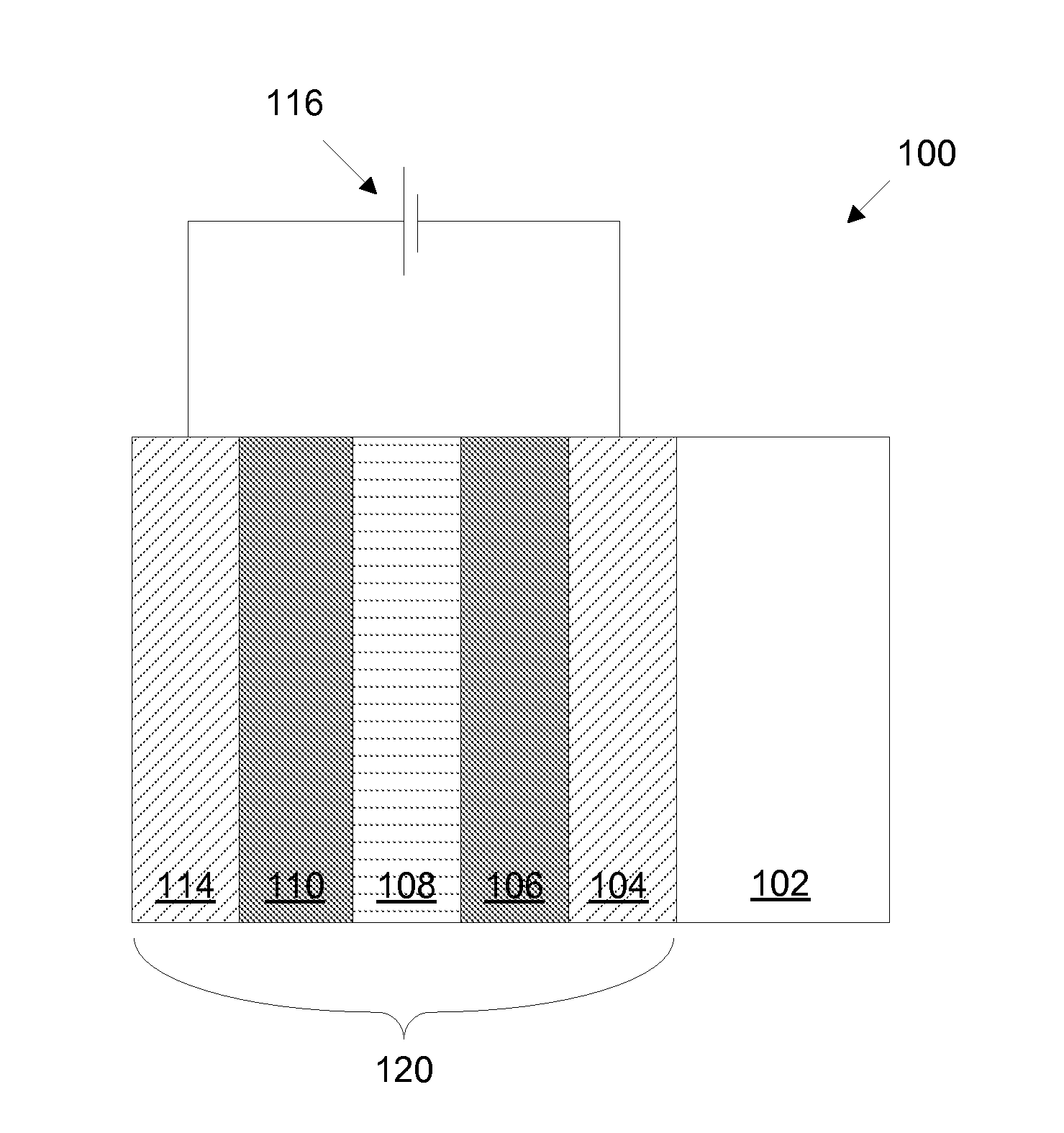
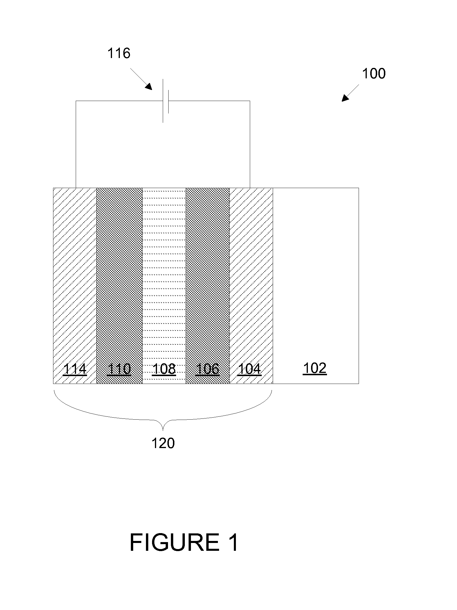
[0028]A schematic cross-section of an electrochromic device 100 in accordance with some embodiments is shown in FIG. 1. The electrochromic device includes a substrate 102, a conductive layer (CL) 104, an electrochromic layer (EC) 106, an ion conducting layer (IC) 108, a counter electrode layer (CE) 110, and a conductive layer (CL) 114. Elements 104, 106, 108, 110, and 114 are collectively referred to as an electrochromic stack 120. A voltage source 116 operable to apply an electric potential across the electrochromic stack 120 effects the transition of the electrochromic device from, e.g., a bleached state to a colored state. In other embodiments, the order of layers is reversed with respect to the substrate. That is, the layers are in the following order: substrate, conductive layer, counter electrode layer, ion conducting layer, electrochromic material layer, conductive layer.

[0029]It should be understood that the reference to a transition between a bleached ...


PUM

PropertyMeasurementUnit
thicknessaaaaaaaaaa
thicknessaaaaaaaaaa
pressureaaaaaaaaaa

Abstract

Prior electrochromic devices frequently suffer from high levels of defectivity. The defects may be manifest as pin holes or spots where the electrochromic transition is impaired. This is unacceptable for many applications such as electrochromic architectural glass. Improved electrochromic devices with low defectivity can be fabricated by depositing certain layered components of the electrochromic device in a single integrated deposition system. While these layers are being deposited and / or treated on a substrate, for example a glass window, the substrate never leaves a controlled ambient environment, for example a low pressure controlled atmosphere having very low levels of particles. These layers may be deposited using physical vapor deposition.

Description

CROSS REFERENCE TO RELATED APPLICATIONS[0001]This application claims the benefit of the earlier filed U.S. provisional application Ser. No. 61 / 165,484, filed Mar. 31, 2009.BACKGROUND[0002]Electrochromism is a phenomenon in which a material exhibits a reversible electrochemically-mediated change in an optical property when placed in a different electronic state, typically by being subjected to a voltage change. The optical property is typically one or more of color, transmittance, absorbance, and reflectance. One well known electrochromic material, for example, is tungsten oxide (WO3). Tungsten oxide is a cathodic electrochromic material in which a coloration transition, transparent to blue, occurs by electrochemical reduction.[0003]Electrochromic materials may be incorporated into, for example, windows and mirrors. The color, transmittance, absorbance, and / or reflectance of such windows and mirrors may be changed by inducing a change in the electrochromic material. One well known ap...

Claims


Application Information

Patent Timeline
Patent Type & Authority Applications(United States)
IPC IPC(8): B05D5/12C23C16/00C23C16/06C23C16/52C23C14/34G02F1/1524
CPCC03C17/3417C03C2217/94C23C10/28C23C14/083C23C14/085G02F1/15C23C14/568C23C14/5806C23C14/5853G02F1/1523B05D5/06C23C14/185C23C14/08C23C14/18C23C14/56C23C14/58G02F1/1524G02F1/1525G02F2001/1536C09K9/00C09K2211/183C09K2211/187B23K20/10C23C14/021C23C14/022C23C14/024C23C14/046C23C14/086C23C14/14C23C14/3407G02F1/1533G02F1/155G02F1/153
Inventor KOZLOWSKI, MARKKURMAN, ERICWANG, ZHONGCHUNSCOBEY, MIKEDIXON, JEREMYPRADHAN, ANSHUROZBICKI, ROBERT
Owner VIEW INC
Learn More