
Power supply circuit and semiconductor device for use therein

a power supply circuit and semiconductor technology, applied in the direction of electric variable regulation, process and machine control, instruments, etc., can solve the problems and achieve the effect of increasing chip size and cos

Active Publication Date: 2010-07-15
ROHM CO LTD
View PDF1 Cites 1 Cited by
  • Summary
  • Abstract
  • Description
  • Claims
  • Application Information

AI Technical Summary

Benefits of technology

[0011]However, the inventor of the present invention has found that the conventional power supply IC 100 described above suffer from the following inconveniences. That is, in the conventional power supply IC 100 described above, since the DC / DC converter and the charge pump are separately formed independent of each other, the transistors M101 and M102, the terminals T101 to T103, and the first driver DRV101 for the DC / DC converter and the transistors M103 to M106, the terminals T104 to T108, and the second driver DRV102 for the charge pump need to be separately prepared. This invites an increase in chip size and a cost increase.
[0012]In view of the above problem, an object of the present invention is to provide a power supply circuit having both a DC / DC converter and a charge pump without an unnecessary increase in number of transistors and external terminals.
[0015]According to the present invention, it is possible to provide a power supply circuit having both a DC / DC converter and a charge pump without an unnecessary increase in number of transistors and external terminals.

Problems solved by technology

This invites an increase in chip size and a cost increase.

Method used


Image

  • Power supply circuit and semiconductor device for use therein
  • Power supply circuit and semiconductor device for use therein
  • Power supply circuit and semiconductor device for use therein

Examples


first embodiment

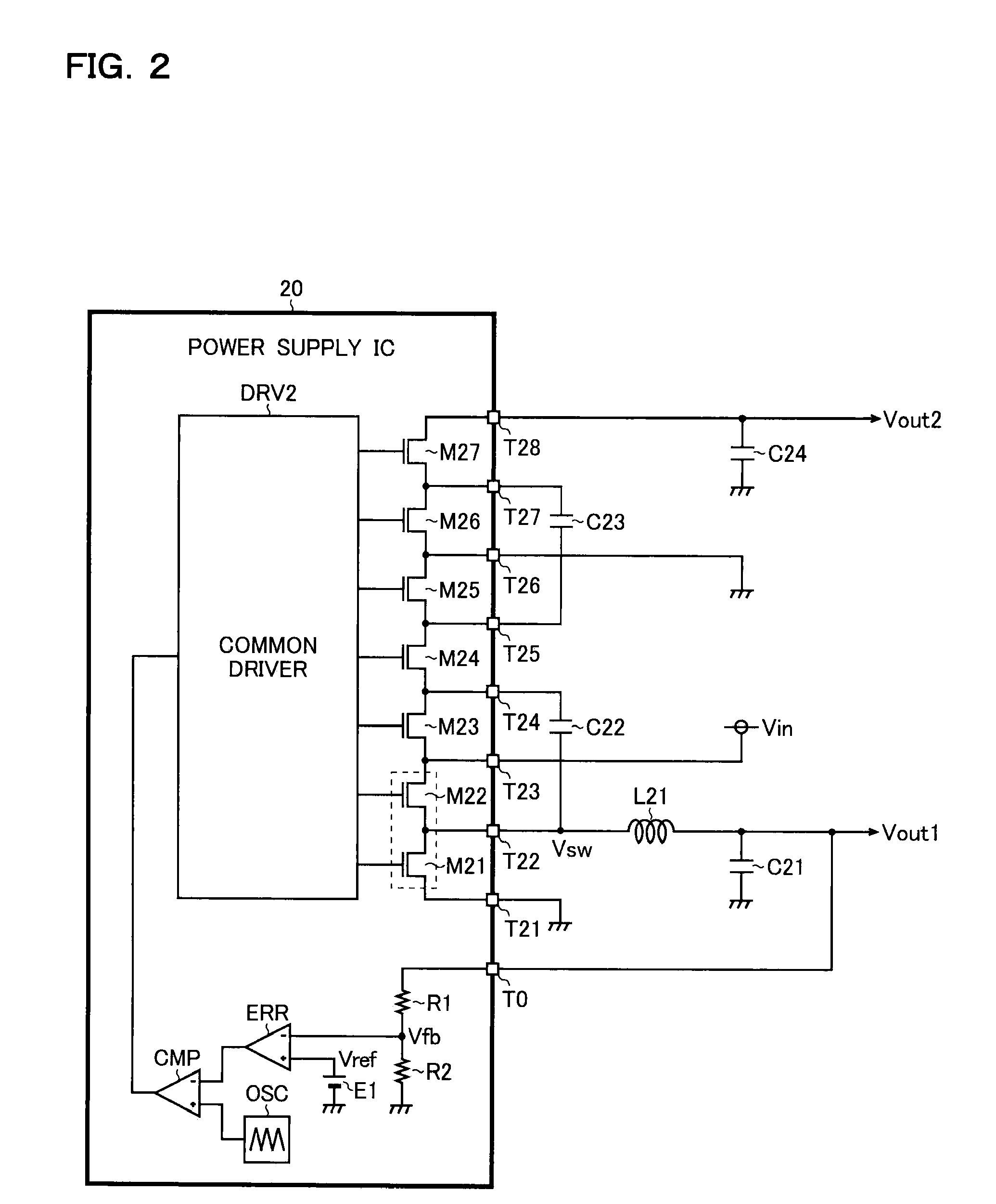
[0041]Inside the power supply IC 20, the transistor M 21 is connected between the terminals T21 and T22. The transistor M22 is connected between the terminals T22 and T23. The transistor M23 is connected between the terminals T23 and T24. The transistor M24 is connected between the terminals T24 and T25. The transistor M25 is connected between the terminals T25 and T26. The transistor M26 is connected between the terminals T26 and T27. The transistor M27 is connected between the terminals T27 and T28. Gates of the transistors M21 to M27 are each connected to the common driver DRV2. The connection relationship among the resistors R1 and R2, the error amplifier ERR, the DC voltage supply E1, the oscillation circuit OSC, the comparator CMP, and the common driver DRV2 is similar to that of the first embodiment described above, and thus no overlapping description thereof will be repeated.

[0042]Outside the power supply IC 20, the terminal T21 is connected to a ground terminal. The termina...

second embodiment

[0054]In the power supply IC 30, the transistor M31 is connected between the terminals T31 and T32. The transistor M32 is connected between the terminals T32 and T33. The transistor M33 is connected between the terminals T33 and T34. The transistor M34 is connected between the terminals T34 and T35. Gates of the transistors M31 to M34 are each connected to the common driver DRV3. The connection relationship among the resistors R1 and R2, the error amplifier ERR, the DC voltage supply E1, the oscillation circuit OSC, the comparator CMP, and the common driver DRV2 is similar to that of the first or second embodiment described above, and thus no overlapping description thereof will be repeated.

[0055]Outside the power supply IC 30, the terminal T31 is connected to a terminal from which an output voltage Vout1 is outputted, and is also connected to a first end of the capacitor C31. A second end of the capacitor C31 is connected to a ground terminal. The terminal T32 is connected to a fir...


PUM


Abstract

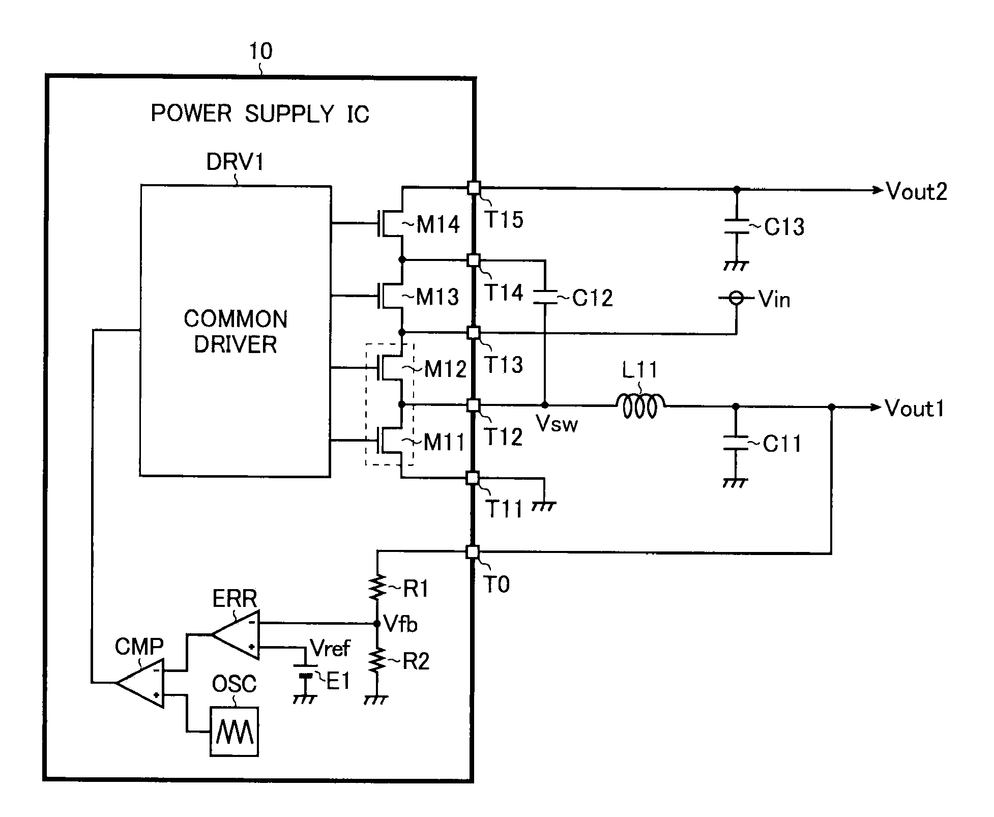
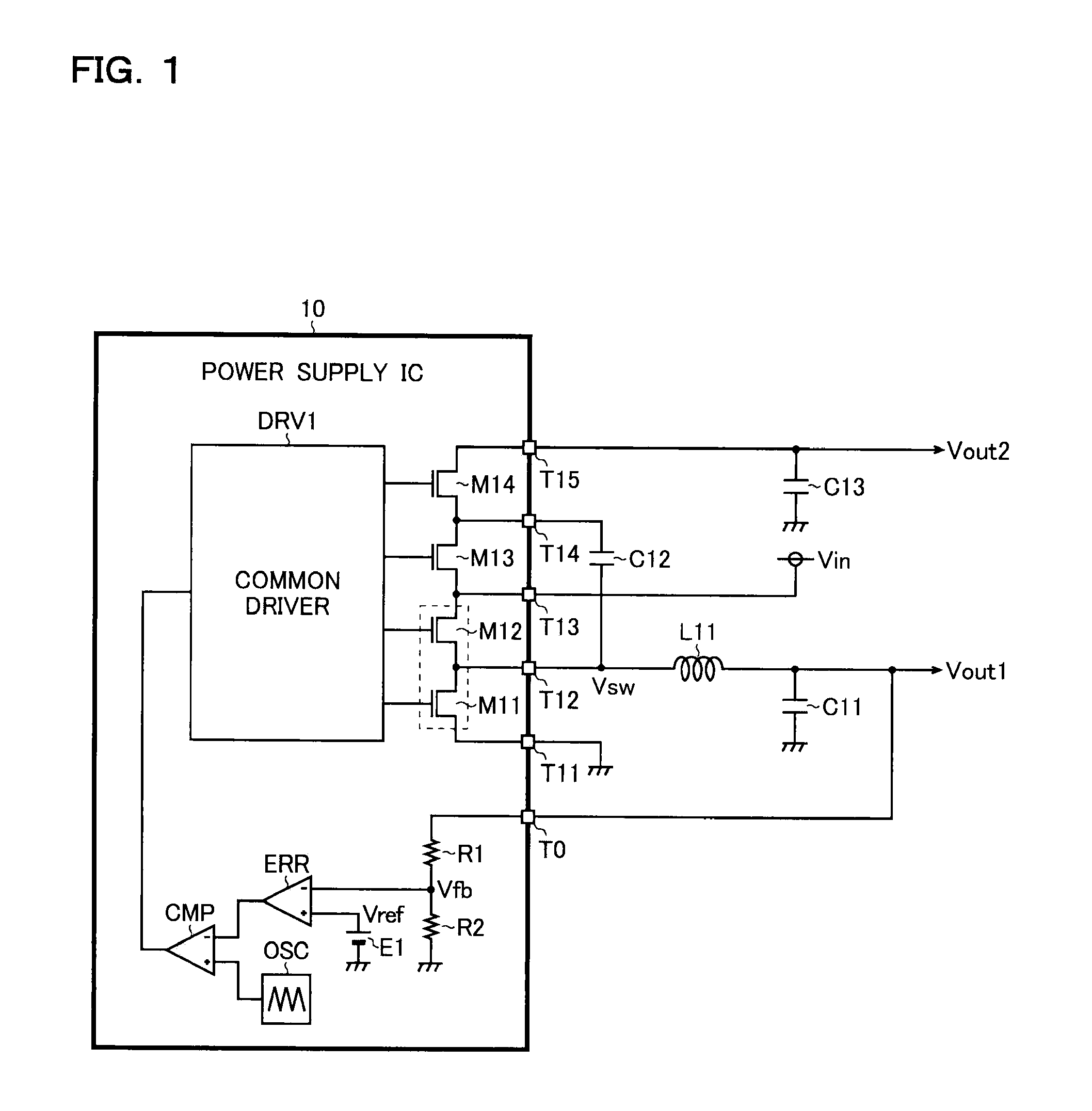
A power supply circuit has: a DC / DC converter (M11, M12, L11, C11) which steps down an input voltage Vin to generate an output voltage Vout1 by rectifying and smoothing a pulsing switched voltage Vsw generated by turning on and off output switches (M11 and M12); and a charge pump (M11-M14, C12, C13) which steps up the input voltage Vin to generate an output voltage Vout2 by repeating charging and discharging of a charge accumulation capacitor (C12) by turning on and off charge transfer switches (M11-M14). First end of the charge accumulation capacitor is connected to a terminal from which the switched voltage Vsw is outputted. The output switches are also used as part of the charge transfer switches.

Description

CROSS-REFERENCE TO RELATED APPLICATIONS[0001]This application is based on Japanese Patent Application No. 2009-2401 filed on Jan. 8, 2008, the contents of which are hereby incorporated by reference.BACKGROUND OF THE INVENTION[0002]1. Field of the Invention[0003]The present invention relates to a power supply circuit that generates a desired output voltage from an input voltage, and a semiconductor device for use therein.[0004]2. Description of Related Art[0005]FIG. 4 is a circuit block diagram showing an example of a conventional power supply circuit. As shown in FIG. 4, the conventional power supply circuit has a power supply IC 100, an inductor L101, and capacitors C101 to C103. The power supply IC 100 has field-effect transistors M101 to M106, first and second drivers DRV101 and DRV102 integrated therein, and further has terminals T101 to T108 as means for establishing external electric connection.[0006]Inside the power supply IC 100, the transistor M101 is connected between the ...

Claims


Application Information

Patent Timeline
IPC IPC(8): G05F1/10
CPCH02M2001/009H02M3/07H02M1/009
Inventor AKAHO, TADASHI
Owner ROHM CO LTD
Learn More