Method for producing a crystalline germanium layer on a substrate

a technology of germanium and crystalline germanium, which is applied in the field of production of gebased layers on a base substrate, can solve the problems of difficult to obtain high-quality crystalline ge on si substrates, high surface roughness, and high crystal quality of ge layers

Active Publication Date: 2010-07-08
INTERUNIVERSITAIR MICRO ELECTRONICS CENT (IMEC VZW) +1
View PDF2 Cites 9 Cited by
  • Summary
  • Abstract
  • Description
  • Claims
  • Application Information

AI Technical Summary

Benefits of technology

[0005]It is an object of embodiments of the present invention to provide a good method for providing a crystalline germanium layer on a base substrate, a method for forming a photovoltaic cell or a photo-electrolysis cell and a method for forming a CMOS device using the method according to embodiments of the invention and a substrate comprising a crystalline germanium layer formed by a method according to embodiments of the invention.

Problems solved by technology

The large lattice mismatch between Ge and Si (4%) makes it difficult to obtain high quality crystalline Ge on Si substrates.
The lattice mismatch leads to a high surface roughness due to island growth and high densities of threading dislocations in the Ge epilayers.
However, the method described in this article did not lead to Ge layers with a high crystal quality.

Method used


Image

  • Method for producing a crystalline germanium layer on a substrate
  • Method for producing a crystalline germanium layer on a substrate
  • Method for producing a crystalline germanium layer on a substrate

Examples


example n357

[0176]For this example, Si(111) substrates were chemically cleaned to remove metal contamination, particles and native oxides. Hereafter a ˜50 nm thick a-Ge (amorphous Ge) was deposited by PECVD on the Si(111) substrates. Then, the substrates were annealed in vacuum at a ˜1e-8 torr background pressure and at a temperature of ˜750° C.

[0177]From the results obtained from these experiments it was found that after deposition, the Ge was amorphous (according to the RHEED (Reflection High Energy Electron Diffraction) measurements). The RHEED results showed streaks during annealing at a temperature of ˜450° C.

[0178]XRD (X-Ray Diffraction) measurements showed a diffraction peak, originating from crystalline Ge, with a omega / 2theta FWHM of 506 arc seconds.

[0179]As a conclusion of this experiment it can be said that a-Ge can be formed by PECVD on Si(111) substrates. This a-Ge can be crystallised when annealed at sufficiently high temperature. It was furthermore found that it was possible to c...

example n362

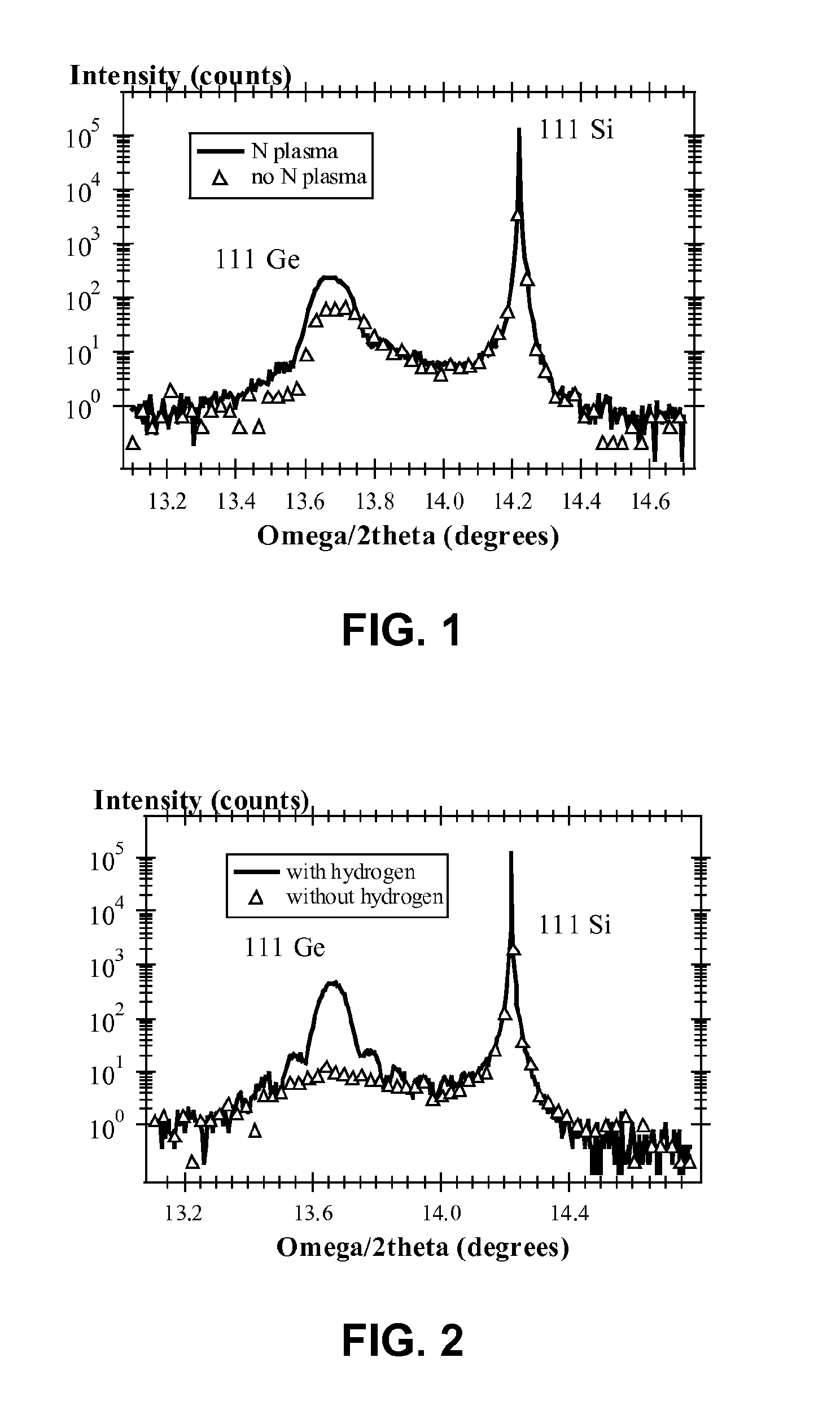
[0180]This experiment was similar to the previous experiment, i.e. example N357, except that now instead of annealing in vacuum, annealing was now performed under N plasma at ˜750° C. (˜2e-5 ton background pressure).

[0181]The Ge peak observed by XRD measurements showed higher intensity than for example N357, indicating better crystal quality in case of the present example. The FWHM (full width at half maximum) was found to be smaller than for example N357: 382 arc seconds (506 arc seconds for example N357), which also indicates better crystal quality in case of the present example. The XRD rocking curve FWHM was 471 arc seconds for the present example and was 665 arc seconds for example N357, which also indicates better crystal quality in case of the present example.

[0182]FIG. 1 shows an XRD Omega / 2theta scan a 50 nm thick crystallised germanium layer on Si(111) comparing the present example with example N357. The solid line shows the result for the present example while the triangl...

example n501-a1

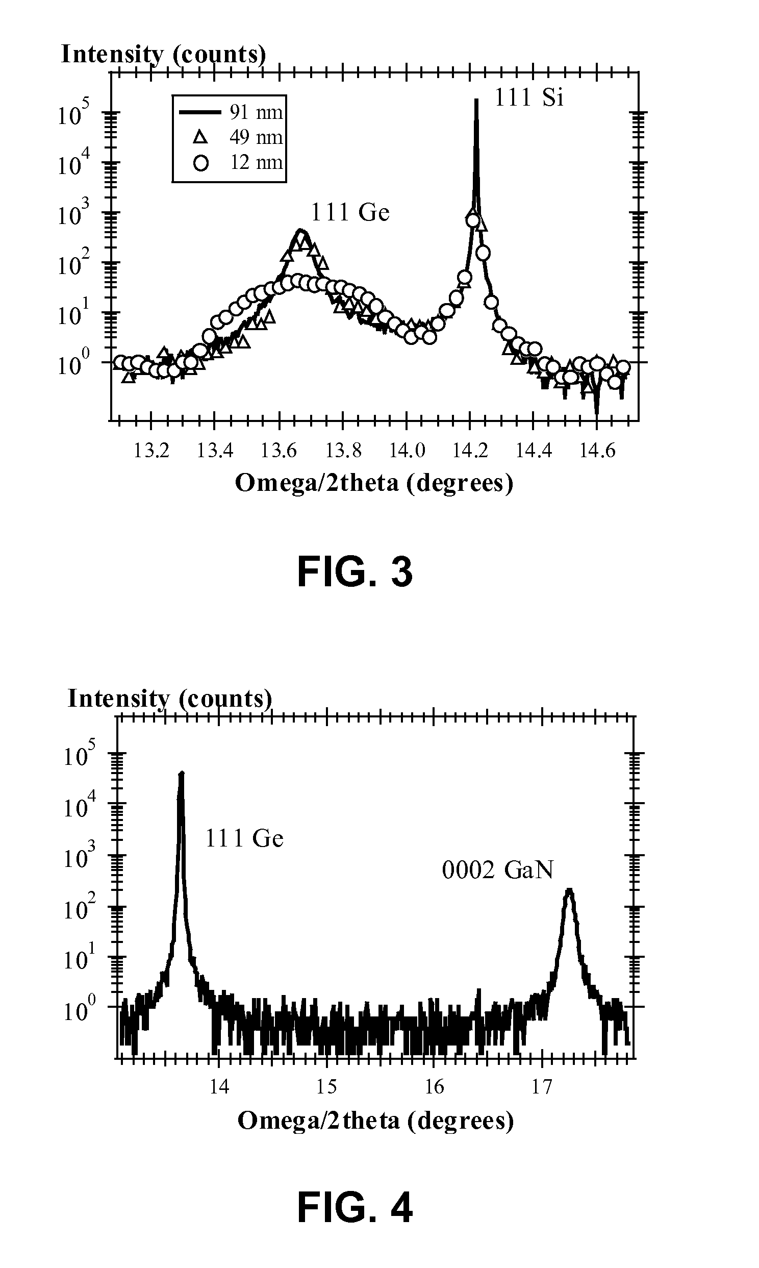
[0214]The present example is similar to example N499-A1, except that in the present example no H2 flow was used during deposition of Ge. The background pressure was around ˜1e-9 torr. Annealing was performed under N2 atmosphere, at a temperature of 600° C. for 1 minute.

[0215]A good Ge peak was observed for example N499-A1. A small peak was observed for the present example (N501-A1). The XRD rocking curve FWHM for example N499-A1 was found to be 287 arc seconds, while it was found to be 958 arc seconds for the present example (N501-A1).

[0216]FIG. 2 shows an XRD Omega / 2theta scan of a crystallised a-Ge layer on Si(111) with (solid line, example N499-A1)) and without (triangles, example N501-A1)) hydrogen being present in the a-Ge layer.

[0217]The surface roughness is comparable for both examples and was found to be around 0.8 nm.

[0218]From these examples it can be concluded that directing a H2 flux onto a sample while depositing a-Ge leads to incorporation of Hydrogen in the a-Ge layer...


PUM

PropertyMeasurementUnit
temperatureaaaaaaaaaa
RMS surface roughnessaaaaaaaaaa
thicknessaaaaaaaaaa

Abstract

The present invention provides a method for providing a crystalline germanium layer on a crystalline base substrate having a crystalline surface. The method comprises cleaning the base substrate for removing contaminants and / or native oxides from the surface, providing an amorphous germanium layer on the surface of the base substrate while exposing to the base substrate to a hydrogen source such as e.g. a hydrogen plasma, a H2 flux or hydrogen originating from dissociation of GeH4 and / or to a non-reactive gas source such as N2, He, Ne, Ar, Kr, Xe, Rn or mixtures thereof, and crystallising the amorphous germanium layer by annealing the base substrate so as to provide a crystalline germanium layer. The present invention also provides a method for the production of a photovoltaic cell or a photo-electrolysis cell or for forming a CMOS device by using the method according to embodiments of the invention and a substrate comprising a crystalline germanium layer formed by a method according to embodiments of the invention.

Description

TECHNICAL FIELD OF THE INVENTION[0001]The present invention relates to the field of semiconductor processing, in particular to the production of Ge-based layers on a base substrate, such as a Si substrate. More particularly, the present invention provides a method for providing a crystalline germanium layer on a base substrate, to a method for forming a photovoltaic cell or a photo-electrolysis cell, a method for forming a CMOS device using the method according to embodiments of the invention and to a substrate comprising a crystalline germanium layer formed by a method according to embodiments of the invention.BACKGROUND OF THE INVENTION[0002]Heteroepitaxy of Ge on Si is a research topic of significant technological importance. Germanium layers integrated into Si-based complementary metal-oxide semiconductor (CMOS) technology offer attractive application possibilities. The large lattice mismatch between Ge and Si (4%) makes it difficult to obtain high quality crystalline Ge on Si s...

Claims


Application Information

Patent Timeline
Patent Type & Authority Applications(United States)
IPC IPC(8): C30B1/02B32B3/00
CPCC23C14/06C23C14/5806C23C16/28C23C16/56C30B1/023C30B29/08Y10T428/24355H01L21/02433H01L21/0245H01L21/02532H01L21/02592H01L21/0262H01L21/02667H01L21/02381
Inventor LIETEN, RUBENDEGROOTE, STEFAN
Owner INTERUNIVERSITAIR MICRO ELECTRONICS CENT (IMEC VZW)
Why Eureka
Try Eureka