Castellated gate MOSFET tetrode capable of fully-depleted operation

a mosfet transistor and channel structure technology, applied in the direction of transistors, semiconductor devices, electrical equipment, etc., can solve the problems of low power consumption of digital functions, under-performing thin-oxide core devices in speed/bandwidth, and reducing the performance of solid-state rf power amplifiers. performance

Active Publication Date: 2010-06-24
IP3 2021 SERIES 600 OF ALLIED SECURITY TRUST I
View PDF1 Cites 14 Cited by
  • Summary
  • Abstract
  • Description
  • Claims
  • Application Information

AI Technical Summary

Benefits of technology

[0012]Moving forward to the semiconductor era, multiple gate arrangements 5 were proposed for Field Effect devices, as shown in FIG. 2, to solve a similar set of problems (U.S. Pat. No. 3,803,461). These prior art FET devices were later utilized in a number of novel RF circuit ...

Problems solved by technology

While CMOS scaling has enabled the circuit and system designer to pack a tremendous amount of functionality onto a silicon die, it has simultaneously created a number of significant problems as far as the chip's ability to interface with the outside world.
Unfortunately, in such technology evolution, the thick oxide I/O device has become somewhat of a “forgotten stepchild”, as only the thin-oxide core devices can truly take advantage of the shrinking feature sizes that are enabled by state-of-the-art photolithography.
More importantly, as the thick oxide device is a “leftover” from the previous technology node, it typically under-performs the thin-oxide core device in terms of speed/bandwidth (ft).
While this reliability-driven voltage trend results in lower power consumption for digital functions, the effect is not necessarily the same in the analog case.
In fact, it has been shown that in an analog-to-digital converter application with a fixed dynamic range requirement, power consumption can actually increase with decreasing power supply.
However, a number of difficulties persist including, in particular, power consumption, cost and scalability.
Bipolar devices consume significantly more power than CMOS devices, which increases package cost and at some point renders them unsuitable as a system solution, in particular for portable devices.
From the standpoint of scaling, bipolar technologies have hit an apparent limit in terms of increasing performance for a given density and power consumption.
The integration of CMOS and bipolar devices (BiCMOS) reduces the ...

Method used


Image

  • Castellated gate MOSFET tetrode capable of fully-depleted operation
  • Castellated gate MOSFET tetrode capable of fully-depleted operation
  • Castellated gate MOSFET tetrode capable of fully-depleted operation

Examples


embodiment 250

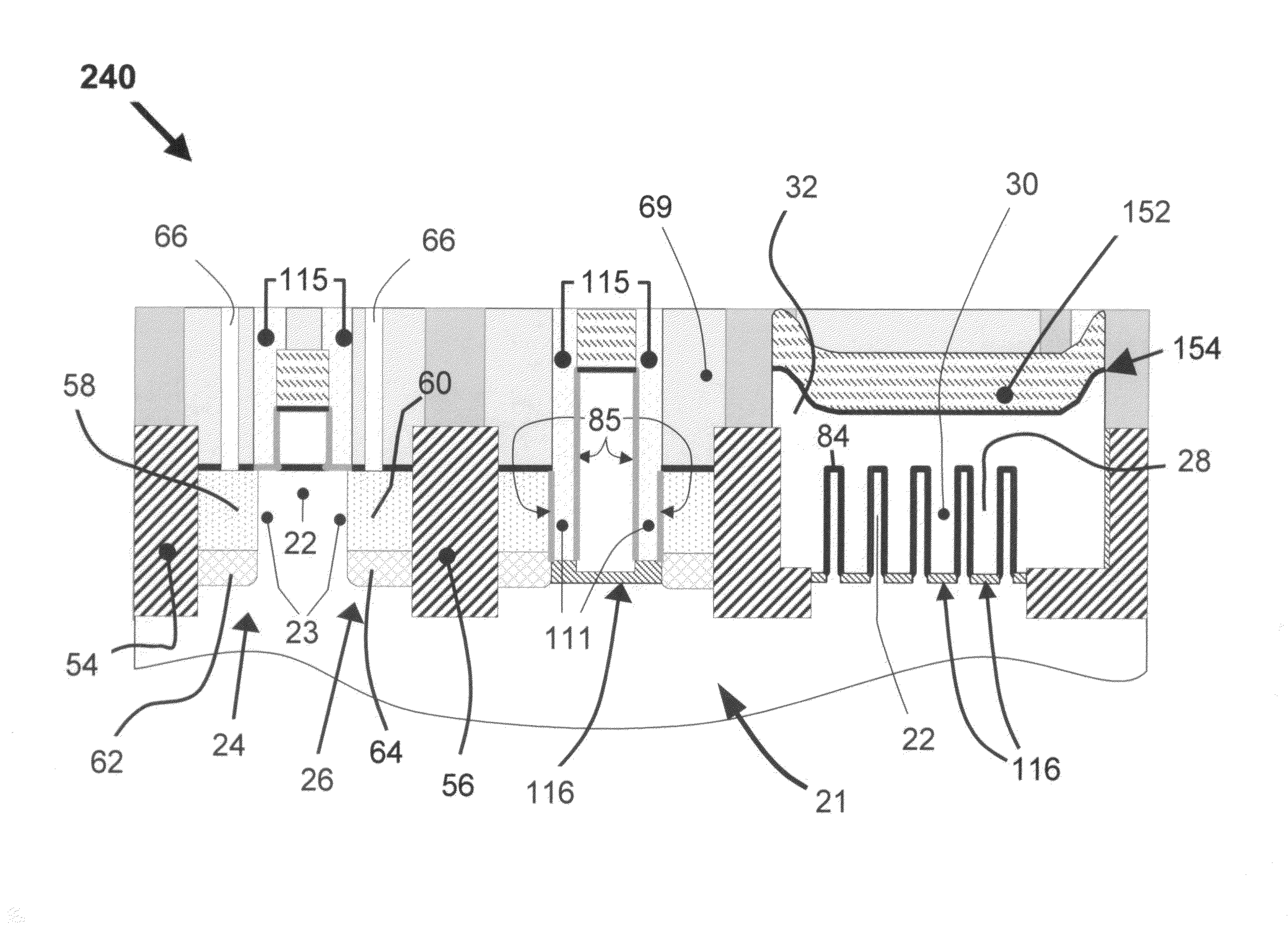
[0069]FIGS. 10 and 10A illustrate a second device embodiment 250 of the disclosed device invention using a starting substrate 78 which has a dielectric layer 77 in a lower portion. A Silicon-On-Insulator (SOI) wafer would be an example of such a starting substrate, and can be produced using a variety of methods. Note that the device mask layout remains substantially the same as the case of the device 240 with the bulk starting wafer 21 shown in FIGS. 9-9A. Substantially similar to the bulk silicon substrate device 240, the device 250 includes a plurality of adjoined primary and secondary silicon channel elements 22,23 that span the distance between a source region 24 and a drain region 26. These primary and secondary channels are controlled by first and second pluralities of gate elements 30,111, respectively, which are separated from the channels using first and second gate dielectrics, 84,85.

[0070]As shown in FIG. 10A, the dielectric layer 77 of device embodiment 250 is spaced bel...

embodiment 260

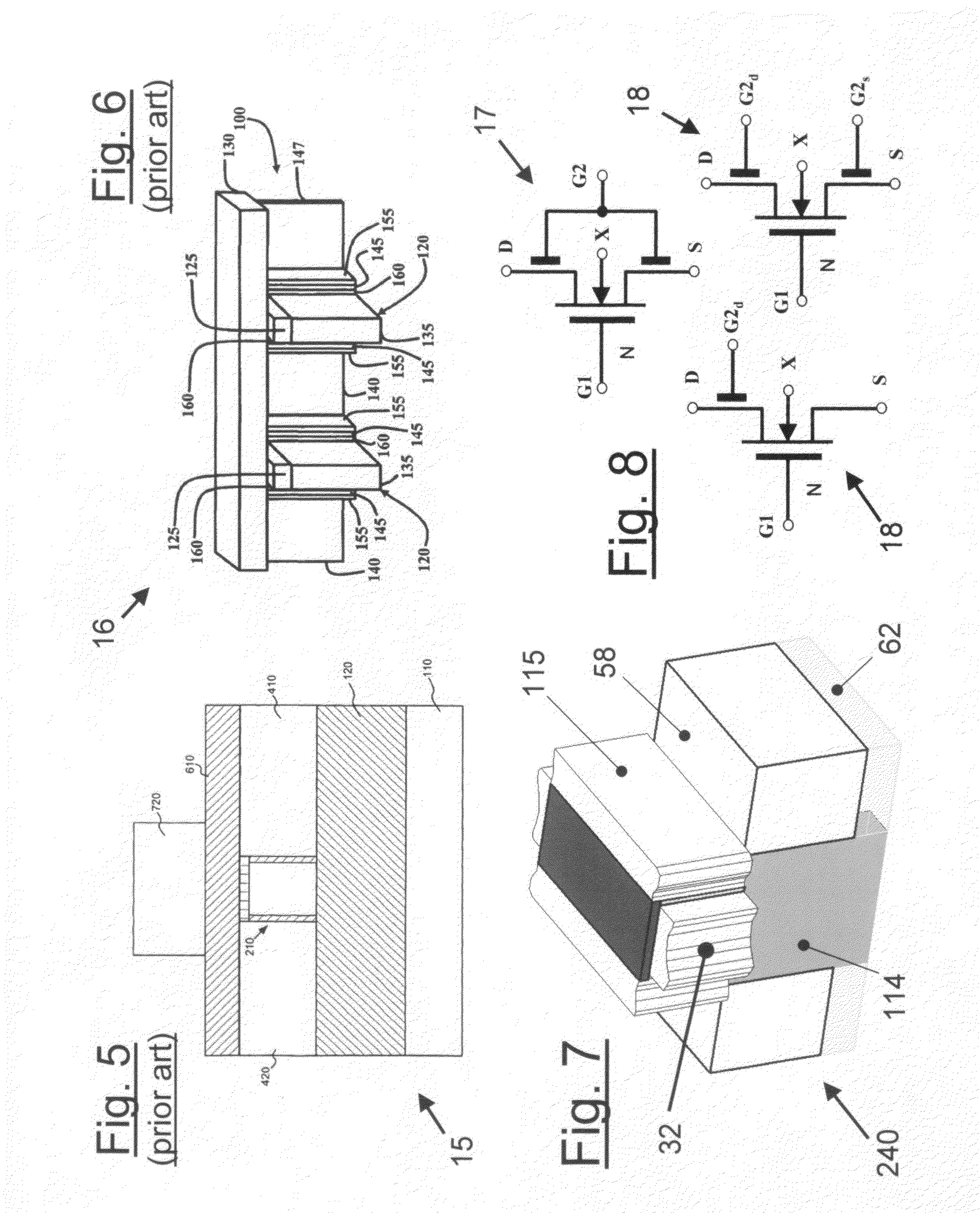
[0082]Contact formation and wiring steps are now performed in the usual manner known in the art to create circuitry, with the resulting final structure illustrated in FIGS. 9 and 9A. It should be noted at this point that if a SOI wafer is used as a starting substrate, the same process steps summarized in FIG. 12, along with masking layers shown in FIG. 9 (and repeated in FIG. 10), are used to create the structure illustrated in FIGS. 10A and 10B. Similarly, the fabrication sequence of FIG. 12 can be used with the spacer formation in procedure 616 omitted to produce the embodiment 260 of FIG. 10C. In this embodiment, the secondary channels of the integrated cascode have been replaced with gated resistors 23′.

Method 2

[0083]Other embodiments of the device constructed in accordance with the present invention can be produced using a second fabrication sequence. In this sequence, a procedure is incorporated whereby a composite gate structure is formed consisting of the first gate, as well...


PUM


Abstract

A castellated-gate MOSFET tetrode device capable of fully depleted operation is disclosed. The device includes a semiconductor substrate region having an upper portion with a top surface and a lower portion with a bottom surface. A source region and a drain region are formed in the semiconductor substrate region, with adjoined primary and secondary channel-forming regions also disposed therein between the source and drain regions, thereby forming an integrated cascade structure. Trench isolation insulator islands, having upper and lower surfaces, surround the source and drain regions as well as the channel-forming regions. Both the primary and secondary channel-forming regions include pluralities of thin, spaced, vertically-orientated semiconductor channel elements that span longitudinally along the device between the source and drain regions. First and second gate structures are provided in the form of pluralities of spaced, castellated first and second gate elements interposed between the primary and secondary channel elements, respectively, with first and second top gate members interconnecting the first and second gate elements at their upper vertical ends to cover the primary and secondary channel elements. The adjoined primary and secondary channel elements are super-self-aligned from the first and second gate elements to the source and drain regions. Finally, first and second dielectric layers separate the primary and secondary channel elements from their respective gate structures.

Description

CROSS REFERENCE TO RELATED APPLICATIONS[0001]This application is a continuation-in-part of co-pending U.S. patent application Ser. No. 11 / 796,652, filed Apr. 27, 2007, to John J. Seliskar, entitled, “A Castellated Gate MOSFET Device Capable of Fully-Depleted Operation”, the contents of which are hereby expressly incorporated herein by reference. Application Ser. No. 11 / 796,652 itself is a continuation-in-part of parent application Ser. No. 10 / 940,093 entitled “An Improved Fully-Depleted Castellated Gate MOSFET Device and Method of Manufacture Thereof”, now U.S. Pat. Nos. 7,212,864 and 7,439,139BACKGROUND OF THE INVENTION[0002]1. Field of the Invention[0003]The present invention relates generally to field effect transistors (FET's) formed as complimentary metal oxide semiconductor (CMOS) structures and, more particularly, to new and improved MOSFET devices having vertically oriented channel structures capable of fully depleted operation. Specifically, the present invention relates to...

Claims


Application Information

Patent Timeline
IPC IPC(8): H01L27/092H01L21/8238
CPCH01L21/845H01L27/1211H01L29/42384H01L29/78636H01L29/66795H01L29/785H01L29/78612H01L29/66545
Inventor SELISKAR, JOHN J.
Owner IP3 2021 SERIES 600 OF ALLIED SECURITY TRUST I
Why Eureka
Try Eureka