Electronic substrate device
- Summary
- Abstract
- Description
- Claims
- Application Information
AI Technical Summary
Benefits of technology
Problems solved by technology
Method used
Image
Examples
first embodiment
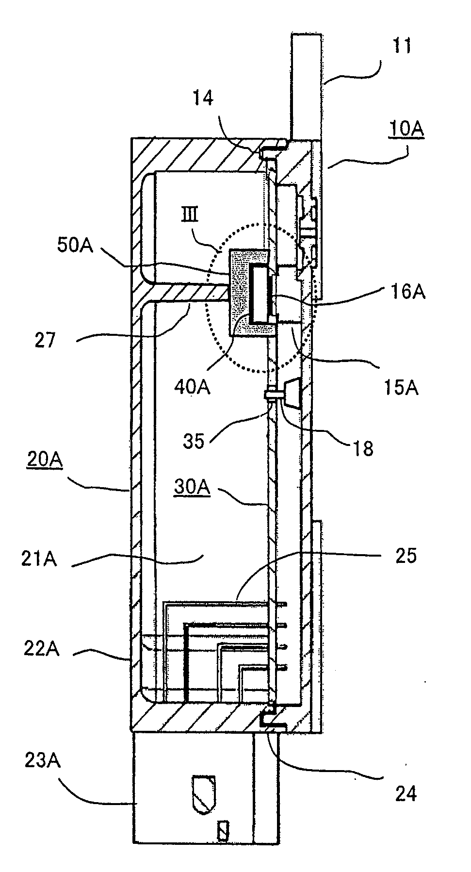
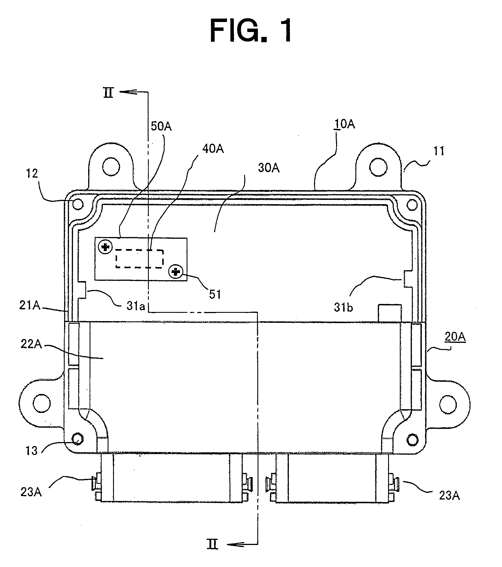
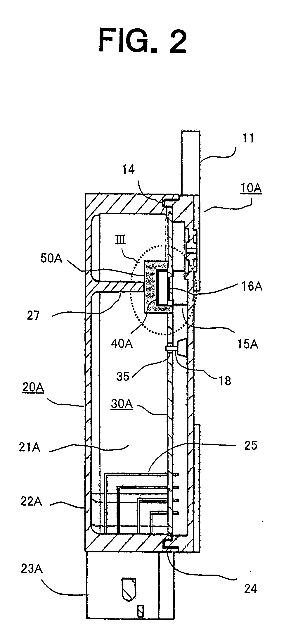
[0026]FIGS. 1 to 3 illustrate an electronic substrate device according to a first embodiment of the present invention. FIG. 1 is a partially cutaway plane view of the electronic substrate device, FIG. 2 is a sectional view taken along the line II-II of FIG. 1, and FIG. 3 is an enlarged view of a main portion III of FIG. 2.
[0027]The electronic substrate device includes a base member 10A serving as a main heat-dissipating member and made by aluminum die casting, an electronic substrate 30A provided on the base member 10A, a heat generating component 40A mounted on the electronic substrate 30A, a heat sink 50A which covers the heat generating component 40A and serves as an auxiliary heat dissipating member, and a cover member 20A which sandwiches the electronic substrate 30A in cooperation with the base member 10A.
[0028]The rectangle base member 10A includes attachment legs 11 protruding on three side surfaces, and the electronic substrate device is fixed to, for example, a wall surfac...
second embodiment
[0076]FIG. 4 is a sectional view of a main portion of an electronic substrate device according to a second embodiment of the present invention.
[0077]In this embodiment, an electronic substrate 30B is disposed in an interior space between the cover member 20A and a base member 10B which is a product molded by aluminum die casting.
[0078]The electronic substrate 30B has a first planar pattern 33a made of copper foil and provided on a rear surface portion thereof, a second planar pattern 33b made of copper foil and provided on a front surface portion opposed to the cover member 20A, and through-holes 34a and 34b which have inner wall surfaces subjected to copper plating and connect the second planar pattern 33b and the first planar pattern 33a so as to transfer heat therebetween.
[0079]The base member 10B has an accommodation recess 15B accommodating a heat generating component 40B through the intermediation of the first gap G1 and a first separated protruding portion 17c which is provid...
third embodiment
[0094]FIG. 5 is a sectional view of a main portion of an electronic substrate device according to a third embodiment of the present invention.
[0095]In this embodiment, an electronic substrate 30C is disposed in an interior space between the cover member 20A and a base member 10C which is a product molded by aluminum die casting.
[0096]In the electronic substrate 30C, a heat generating component 40C is mounted to the rear surface portion on the base member 10C side.
[0097]The heat generating component 40C serving as the heat generating element has a die pad 42C having an exposed surface 44C, an electronic component 41C which is a heat generating element attached to the die pad 42C, and a plurality of connecting terminals 43c electrically connected by soldering to the wiring patterns of the rear surface portion of the electronic substrate 30C.
[0098]The base member 10C has an accommodation recess 15C accommodating the heat generating component 40C through the intermediation of the first ...
PUM
 Abstract
Description
Claims
Application Information
 - R&D
- Intellectual Property
- Life Sciences
- Materials
- Tech Scout
- Unparalleled Data Quality
- Higher Quality Content
- 60% Fewer Hallucinations
Browse by: Latest US Patents, China's latest patents, Technical Efficacy Thesaurus, Application Domain, Technology Topic, Popular Technical Reports.
© 2025 PatSnap. All rights reserved.Legal|Privacy policy|Modern Slavery Act Transparency Statement|Sitemap|About US| Contact US: help@patsnap.com


