
Purification process for semiconducting monomers

Inactive Publication Date: 2010-05-13
XEROX CORP
View PDF4 Cites 13 Cited by
  • Summary
  • Abstract
  • Description
  • Claims
  • Application Information

AI Technical Summary

Benefits of technology

[0042]Polymers made using the monomers of Formula (II) that are purified using the processes of the present disclosure have higher mobility. In embodiments, they have a mobility of 0.2 cm2/V·or greater. The polymer may also

Problems solved by technology

In addition, the mobilities were difficult to reproduce.
This difficulty in reproducibility and low mobility may be attributed to impurities in the polymers, which arise from impurities in the monomer used to form the polymers.

Method used


Image

  • Purification process for semiconducting monomers
  • Purification process for semiconducting monomers
  • Purification process for semiconducting monomers

Examples


example 1

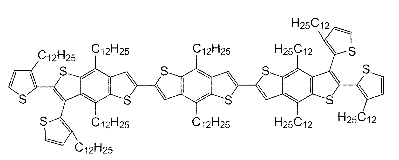
[0066]A PBTBT-12 polymer was made according to the processes of the present disclosure.

[0067]Synthesis of Monomer 3:

[0068]2,6-dibromo-4,8-didodecylbenzo[1,2-b;4,5;b′]dithiophene 1 was prepared as described in Chem. Mater., 2006, Vol. 18, No. 14, pp. 3237-41, the disclosure of which is totally incorporated herein by reference.

[0069]3-dodecylthiophene-2-boronic acid pinacol ester 2 was prepared as described in U.S. Patent Publication No. 2008 / 0103286, the disclosure of which is totally incorporated herein by reference.

[0070]2.0 grams of dithiophene 1, 2.76 grams of pinacol ester 2, and 25 mL of toluene were added to a 250 mL 3-necked reaction flask. The resulting mixture was thoroughly stirred and was purged with argon. Next, 0.07 grams of tetrakis(triphenylphosphine palladium(0)) (Pd(Ph3P)4), 0.72 grams of ALIQUAT® in 10 mL toluene, and 8.4 mL of 2 M aqueous Na2CO3 was added to the mixture. The reaction mixture obtained was stirred at 105° C. for 72 hours. After cooling to room tempe...


PUM

PropertyMeasurementUnit
Fractionaaaaaaaaaa
Fractionaaaaaaaaaa
Melting pointaaaaaaaaaa

Abstract

Disclosed is a process for purifying monomers of Formula (II): wherein R1 and R2 are independently selected from alkyl, substituted alkyl, aryl, substituted aryl, alkoxy, substituted alkoxy, and halogen; and R′ is selected from hydrogen, alkyl, substituted alkyl, aryl, substituted aryl, alkoxy, substituted alkoxy, and halogen. After the monomer is synthesized, it is purified by column chromatography using neutral alumina and hexane as an eluent. The resulting product can also be further recrystallized using isopropanol, hexane, heptane, or toluene. Polymers formed from the purified monomer exhibit higher mobility and increased reproducibility of the mobility.

Description

BACKGROUND[0001]The present disclosure relates, in various embodiments, to processes for purifying compositions used in electronic devices, such as thin film transistors (“TFT”s). The present disclosure also relates to the components or layers produced using such compositions and processes, as well as electronic devices containing such materials.[0002]Thin film transistors (TFTs) are fundamental components in modern-age electronics, including, for example, sensors, image scanners, and electronic display devices. It is generally desired to make TFTs which have not only much lower manufacturing costs, but also appealing mechanical properties such as being physically compact, lightweight, and flexible.[0003]TFTs are generally composed of a supporting substrate, three electrically conductive electrodes (gate, source and drain electrodes), a channel semiconducting layer, and an electrically insulating gate dielectric layer separating the gate electrode from the semiconducting layer. In o...

Claims


Application Information

Patent Timeline
IPC IPC(8): C08F4/26C07D333/50C08F28/06
CPCC07D333/50C08G61/126C08G2261/124C08G2261/1424H01L51/0025C08G2261/3243C08G2261/43C08G2261/51C08G2261/92C08G2261/3223H10K71/311
Inventor LI, YUNINGLIU, PINGWU, YILIANG
Owner XEROX CORP
Learn More