Semiconductor memory for disconnecting a bit line from sense amplifier in a standby period and memory system including the semiconductor memory
a technology of semiconductor memory and memory cells, which is applied in the direction of information storage, static storage, digital storage, etc., can solve the problems of no method of reducing the leak current accompanying the short circuit between a word line and a bit line in a shared sense amplifier type semiconductor memory, and achieves the prevention of wasteful operation of the connection switch, easy identification, and reduced leak current
- Summary
- Abstract
- Description
- Claims
- Application Information
AI Technical Summary
Benefits of technology
Problems solved by technology
Method used
Image
Examples
first embodiment
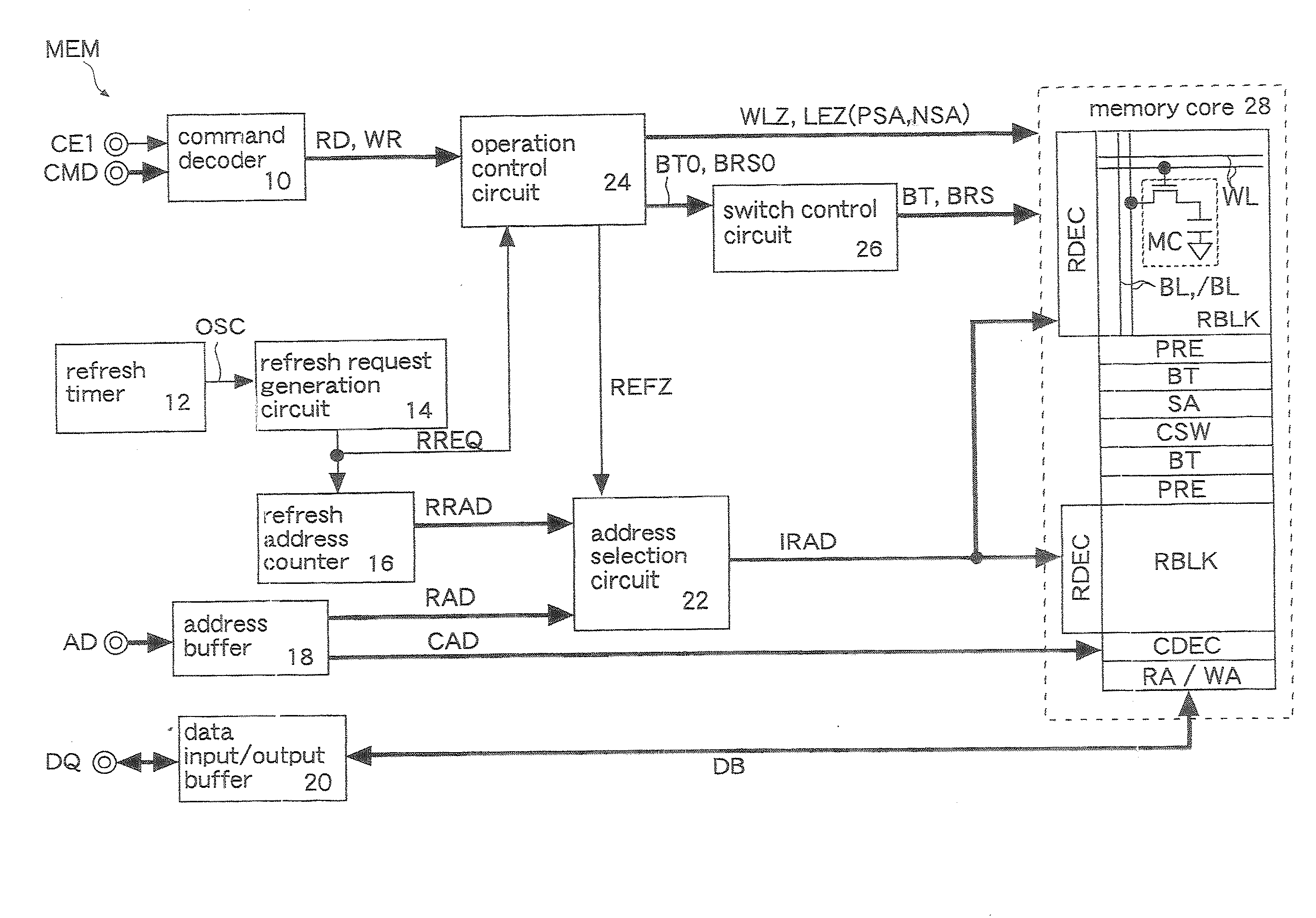
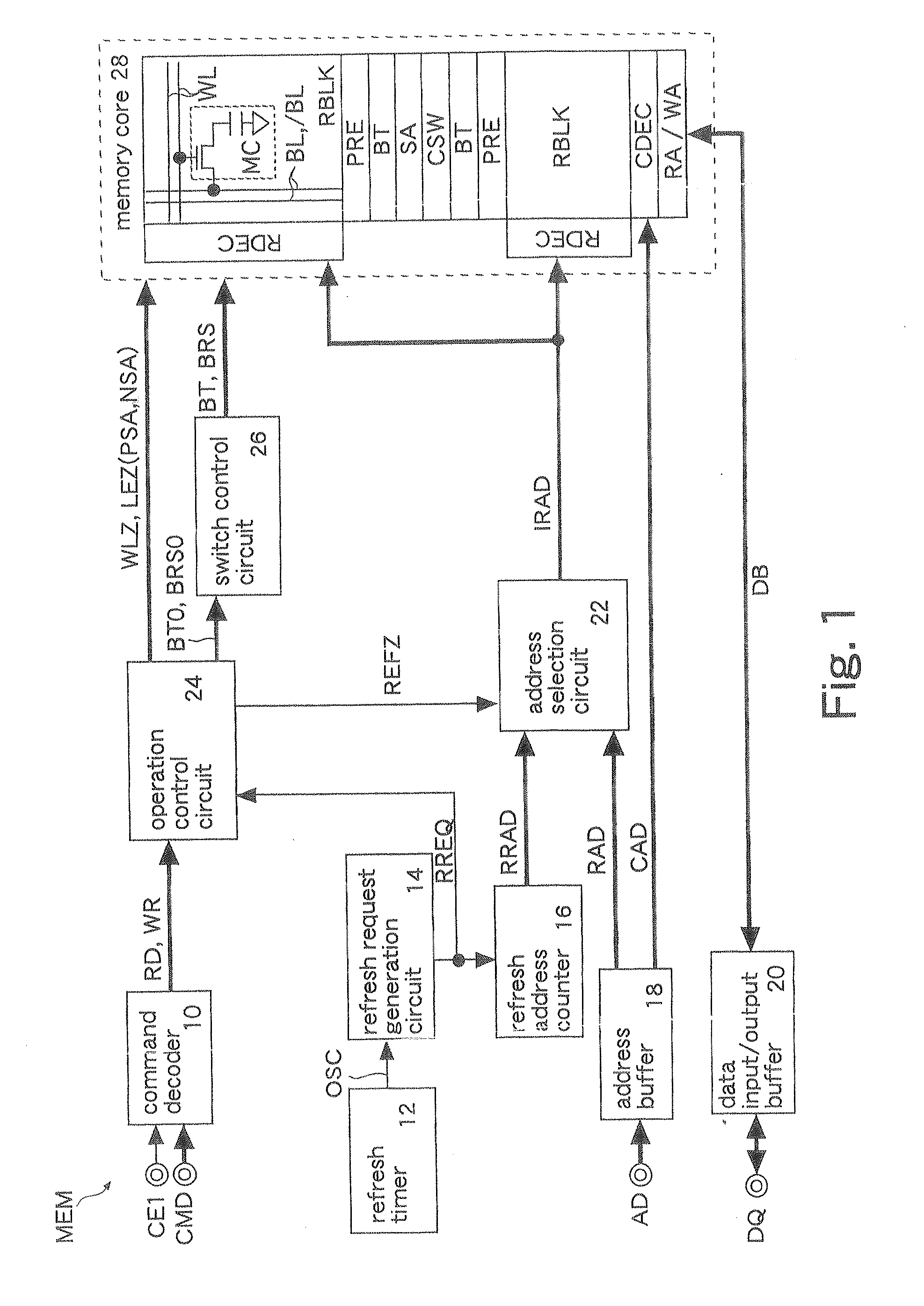
[0090]FIG. 1 shows the present invention. A semiconductor memory MEM is, for example, an FCRAM (Fast Cycle RAM). The FCRAM is a pseudo SRAM having memory cells of DRAM and an interface of SRAM. The memory MEM has a command decoder 10, a refresh timer 12, a refresh request generation circuit 14, a refresh address counter 16, an address buffer 18, a data input / output buffer 20, an address selection circuit 22, an operation control circuit 24, a switch control circuit 26, and a memory core 28. The memory MEM constitutes, as shown in FIG. 4 described later, a memory system together with a CPU.
[0091]The command decoder 10 outputs a command recognized in accordance with logical levels of a chip enable signal CE1 and a command signal CMD as a read command RD, a write command WR or the like for performing an access operation of the memory core 28. The read command RD and write command WR are external access requests for performing an access operation to the memory core 28. For example, the ...
sixth embodiment
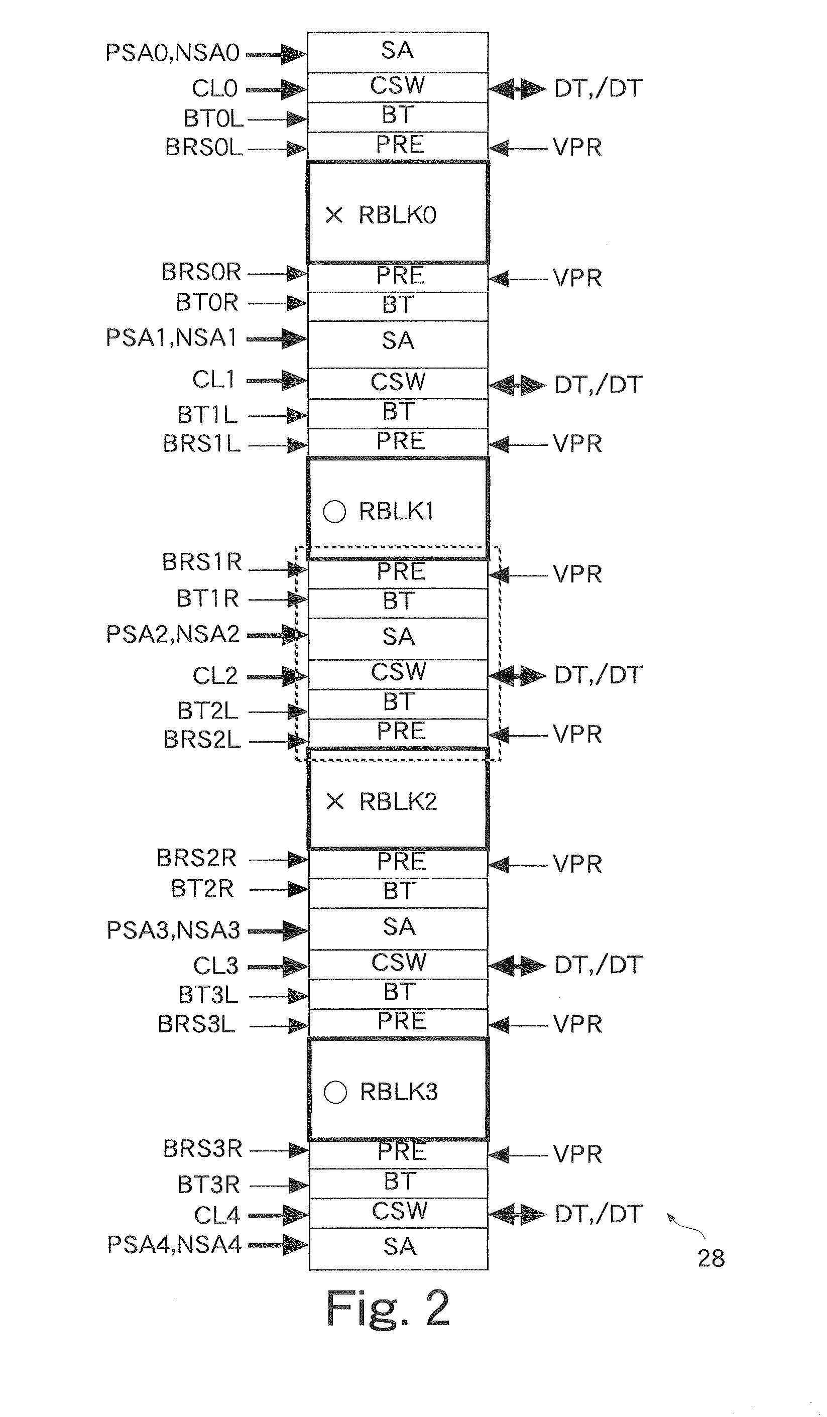
[0138]Also in the sixth embodiment described above, the same advantages as those of the above embodiments can be obtained. Further, in the present embodiment, a precharge operation of the bit lines BL and / BL can be performed for each refresh request RREQ in all bad memory blocks RBLK0 and 2 by releasing the cutoff function for all bad memory blocks RBLK0 and 2 for each refresh request RREQ. This can minimize a shift of the bit lines BL and / BL in the self-refresh period SREFP.
[0139]FIG. 15 shows operations of a seventh embodiment. The same symbols and numerals are attached to the same components as those described in the above embodiments and a detailed description thereof is omitted. In the present embodiment, the cutoff function to turn off the connection switch BT is set in a period in which no access operation RD or WR is performed in the activation period ACTP. Other components are the same as those in the sixth embodiment (FIG. 14). A memory MEM in the present embodiment is t...
tenth embodiment
[0146]Also in the tenth embodiment described above, the same advantages as those of the above embodiments can be obtained. Further, in the present embodiment, the cutoff function can be prevented from immediately being released after being set when the chip enable signal CE1 is temporarily inactivated. In other words, the cutoff function can be set after reliably entering the self-refresh mode by waiting until refresh requests RREQ occur a predetermined number of times before the cutoff function is set. As a result, the switch control circuit 26F can be prevented from repeatedly setting / releasing the cutoff function wastefully, thereby reducing current consumption of the memory MEM.
[0147]FIG. 20 shows an eleventh embodiment of the present invention. The same symbols and numerals are attached to the same components as those described in the above embodiments and a detailed description thereof is omitted. In the present embodiment, a switch control circuit 26G is formed instead of the...
PUM
 Abstract
Description
Claims
Application Information
 - R&D
- Intellectual Property
- Life Sciences
- Materials
- Tech Scout
- Unparalleled Data Quality
- Higher Quality Content
- 60% Fewer Hallucinations
Browse by: Latest US Patents, China's latest patents, Technical Efficacy Thesaurus, Application Domain, Technology Topic, Popular Technical Reports.
© 2025 PatSnap. All rights reserved.Legal|Privacy policy|Modern Slavery Act Transparency Statement|Sitemap|About US| Contact US: help@patsnap.com


