Semiconductor Device and Method of Fabricating the Same

Inactive Publication Date: 2010-03-25
DONGBU HITEK CO LTD
View PDF8 Cites 10 Cited by
  • Summary
  • Abstract
  • Description
  • Claims
  • Application Information

AI Technical Summary

Benefits of technology

[0005]A method of fabricating a semiconductor device is provided that can reduce the deviation between semiconductor devices. In addition, an embodiment of the present invention provides a flash memory device that can be highly integrated and a method of driving the same.

Problems solved by technology

However, because the flash memory devices further include the select transistor, it can be difficult to obtain high integration.

Method used


Image

  • Semiconductor Device and Method of Fabricating the Same
  • Semiconductor Device and Method of Fabricating the Same
  • Semiconductor Device and Method of Fabricating the Same

Examples


Embodiment Construction

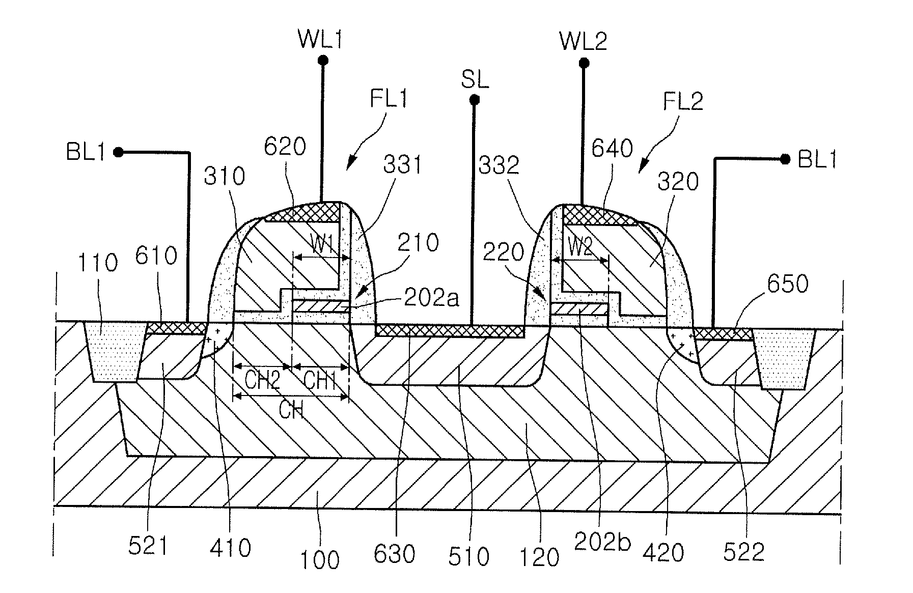
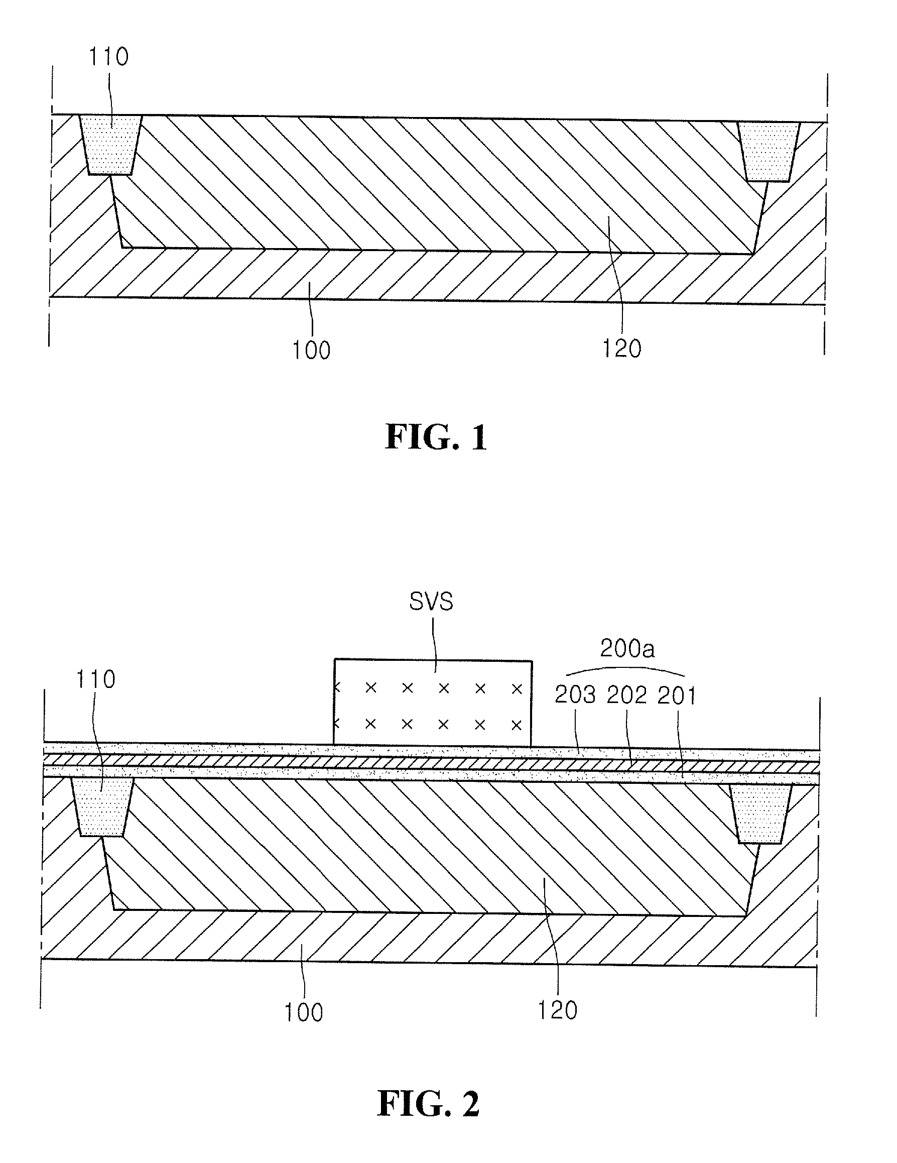
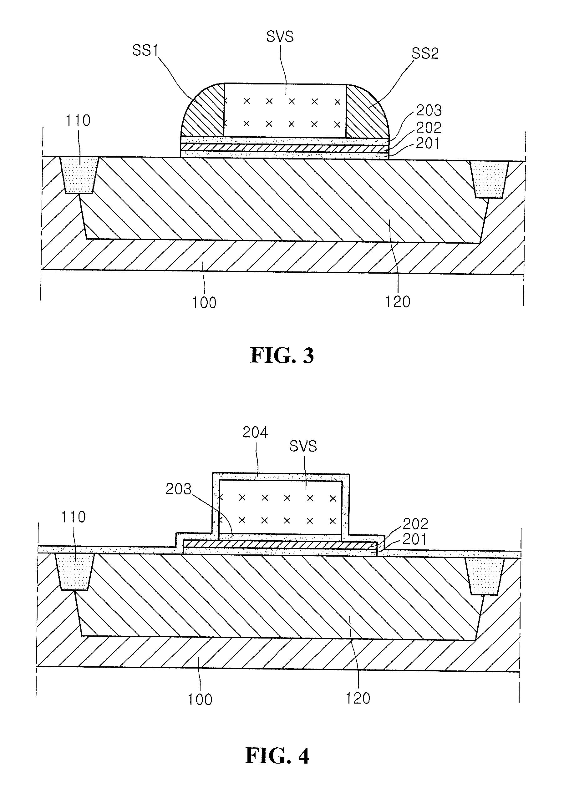
[0023]When the terms “on” or “over” are used herein, when referring to layers, regions, patterns, or structures, it is understood that the layer, region, pattern or structure can be directly on and in contact with another layer or structure, or intervening layers, regions, patterns, or structures may also be present. When the terms “under” or “below” are used herein, when referring to layers, regions, patterns, or structures, it is understood that the layer, region, pattern or structure can be directly under and in contact with the other layer or structure, or intervening layers, regions, patterns, or structures may also be present. Also, being “on” or “under” each layer will be described based on the drawings. In the drawings, the thickness or size of each layer may be exaggerated, omitted or schematically illustrated for the convenience and clarity of explanation. Also, the size of each element in the figures does not completely reflect its actual size.

[0024]FIGS. 1 to 7 are cross...


PUM


Abstract

A method of fabricating a semiconductor device and a flash memory device are provided. The method of fabricating the semiconductor device includes: forming a nitride film on a semiconductor substrate; forming a sacrificial vertical structure on the nitride film; forming sacrificial spacers on lateral surfaces of the sacrificial vertical structure; performing an initial patterning of the nitride film using the sacrificial vertical structure and the sacrificial spacers as etch masks; removing the sacrificial spacers after the initial patterning of the nitride film and forming gate electrodes on the lateral surfaces of the sacrificial vertical structure; and removing the sacrificial vertical structure from between the gate electrodes and performing a secondary patterning of the nitride film using the gate electrodes as etch masks.

Description

CROSS-REFERENCE TO RELATED APPLICATIONS[0001]This application claims the benefit under 35 U.S.C. §119 of Korean Patent Application Nos. 10-2008-0092600, filed Sep. 22, 2008, and 10-2008-0109772, filed Nov. 6, 2008, which are hereby incorporated by reference in their entirety.BACKGROUND[0002]The present disclosure relates to a method of fabricating a semiconductor device, and a flash memory device and a method of driving the same.[0003]With the development in information processing technology, high-integrated flash memory devices have been developed. In particular, flash memory devices having a Silicon-Oxide-Nitride-Oxide-Silicon (SONOS) structure have been developed.[0004]Such flash memory devices may include a select transistor for preventing an over-erase. However, because the flash memory devices further include the select transistor, it can be difficult to obtain high integration.BRIEF SUMMARY[0005]A method of fabricating a semiconductor device is provided that can reduce the de...

Claims


Application Information

Patent Timeline
IPC IPC(8): G11C16/04H01L21/28H01L29/792
CPCG11C16/0425G11C16/3486H01L29/792H01L29/4234H01L27/11568H10B43/30
Inventor JOO, SUNG JOONG
Owner DONGBU HITEK CO LTD
Why Eureka
Try Eureka