Semiconductor memory device and driving method thereof

a memory device and semiconductor technology, applied in the direction of information storage, static storage, digital storage, etc., can solve the problems of reducing the reliability of internal data signals, reducing mass production and compatibility of products, and not maintaining the slew rate, so as to achieve the effect of maintaining the same operational characteristics

Active Publication Date: 2010-03-11
SK HYNIX INC
View PDF2 Cites 9 Cited by
  • Summary
  • Abstract
  • Description
  • Claims
  • Application Information

AI Technical Summary

Benefits of technology

[0030]Another embodiment of the present invention is directed to providing a semiconductor memory device capable of ensuring that data being input to or output from the input and output circuits can reliably have the same operational characteristics regardless of the external power supply voltage.

Problems solved by technology

This inconstant duty ratio results in a reduction in reliability of the internal data signal.
However, the cases illustrated in (B) and (C) of FIG. 3 do not maintain the slew rate.
Moreover, since the current being consumed exists outside of the range defined in the spec, mass-production and compatibility of products can be decreased.
That is, if the products manufactured do not meet the spec, they are dealt with as being defective, thus lowering the efficiency of mass-production.

Method used


Image

  • Semiconductor memory device and driving method thereof
  • Semiconductor memory device and driving method thereof
  • Semiconductor memory device and driving method thereof

Examples


Embodiment Construction

[0046]Hereinafter, preferred embodiments of the present invention will be described in detail with reference to the accompanying drawings so that the invention can readily be practiced by those skilled in the art.

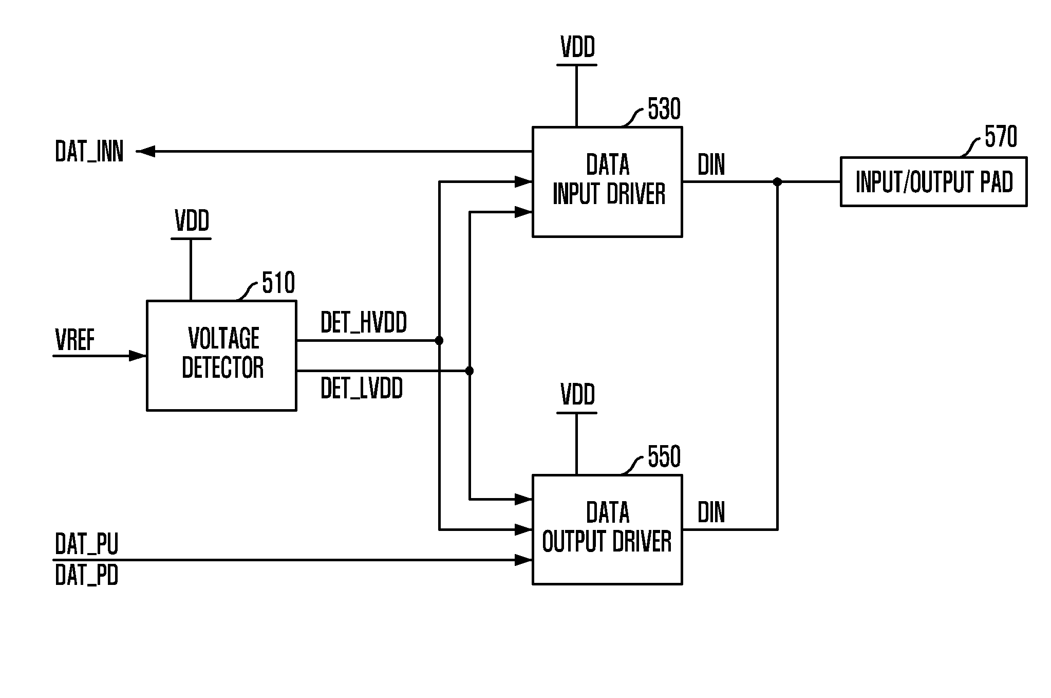
[0047]FIG. 5 is a block diagram illustrating a partial configuration for explaining a semiconductor memory device in accordance with an embodiment of the present invention.

[0048]Referring to FIG. 5, the semiconductor memory device includes a voltage detector 510, a data input driver 530, a data output driver 550, and an input / output pad 570.

[0049]The voltage detector 510 serves to detect a voltage level of an external power supply voltage VDD to generate first and second detection signals DET_HVDD and DET_LVDD in response to the external power supply voltage VDD and an external reference voltage VREF. The external reference voltage VREF is a voltage which is provided from the outside and has, for example, a ½ level of the external power supply voltage VDD applied to the sem...


PUM


Abstract

A semiconductor memory device includes a data input driver and a data output driver for receiving an external power supply voltage, and for inputting and outputting data, respectively; and a voltage detector for detecting the external power supply voltage to generate a detection signal, wherein a drive current of each of the data input driver and the data output driver is controlled by the detection signal.

Description

CROSS-REFERENCE TO RELATED APPLICATION[0001]The present invention claims priority of Korean patent application number 10-2008-0089297, filed on Sep. 10, 2008, which is incorporated by reference in its entirety.BACKGROUND OF THE INVENTION[0002]The present invention relates to a semiconductor design technology, and more particularly, to a semiconductor memory device provided with a data input driver and a data output driver for inputting and outputting data, respectively, and a driving method thereof.[0003]In general, a semiconductor memory device, including Double Data Rate Synchronous RAM (DDR SDRAM), stores or outputs data in accordance with a command required by a Central Processing Unit (CPU). If a write command is provided from the CPU, data from the outside is stored in a memory cell corresponding to an address required by the CPU, and if a read command is provided from the CPU, data stored in a memory cell corresponding to an address required by the CPU is outputted to the out...

Claims


Application Information

Patent Timeline
IPC IPC(8): G11C7/00G11C5/14G11C8/08
CPCG11C5/143G11C7/1051G11C7/1057G11C11/4093G11C7/1078G11C7/1084G11C11/4074G11C7/1066G11C5/14G11C7/10
Inventor KIM, KI-HOLEE, KANG-SEOL
Owner SK HYNIX INC
Why Eureka
Try Eureka