Measurement circuit for an electronic ballast
- Summary
- Abstract
- Description
- Claims
- Application Information
AI Technical Summary
Benefits of technology
Problems solved by technology
Method used
Image
Examples
first embodiment
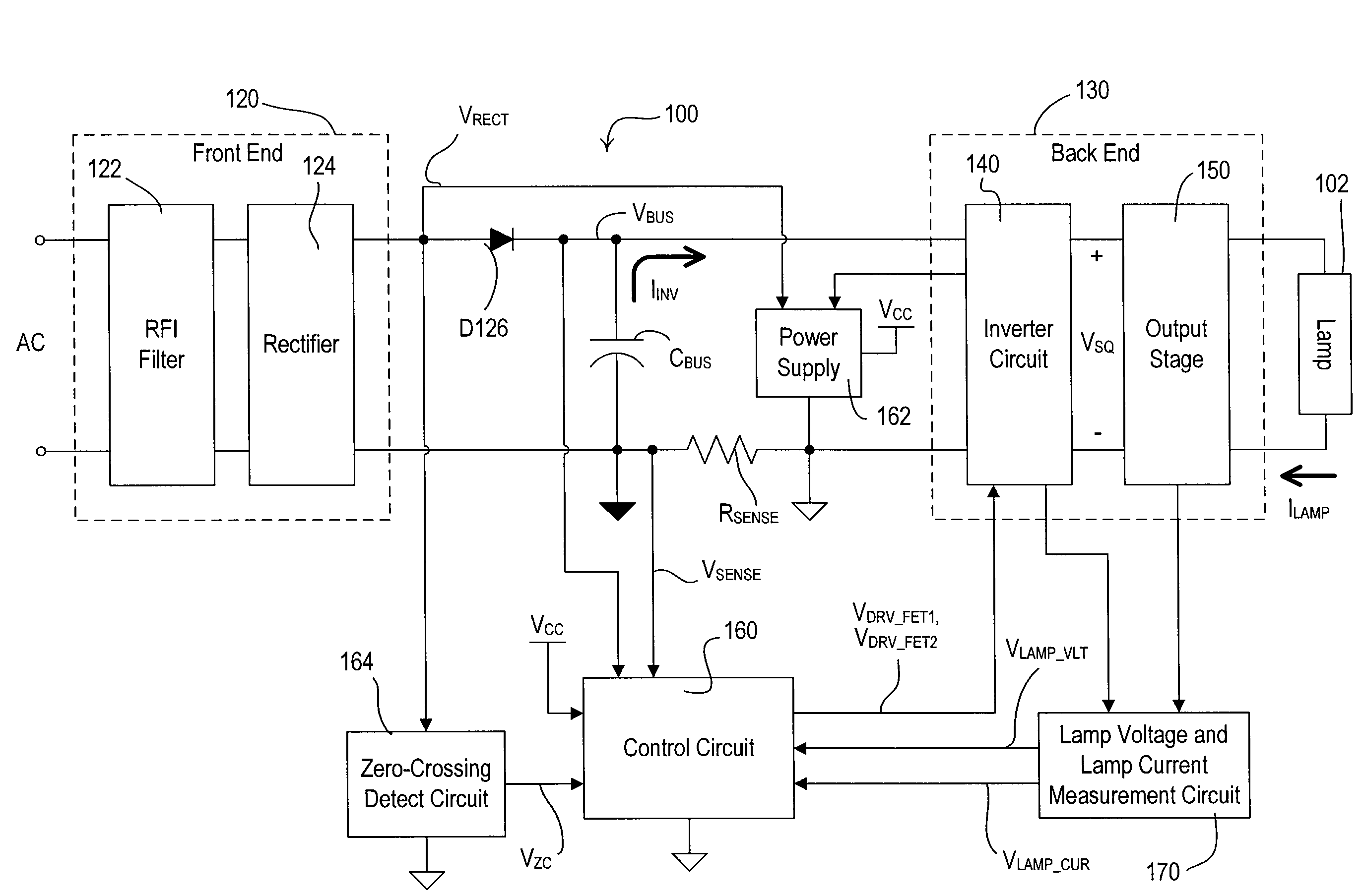
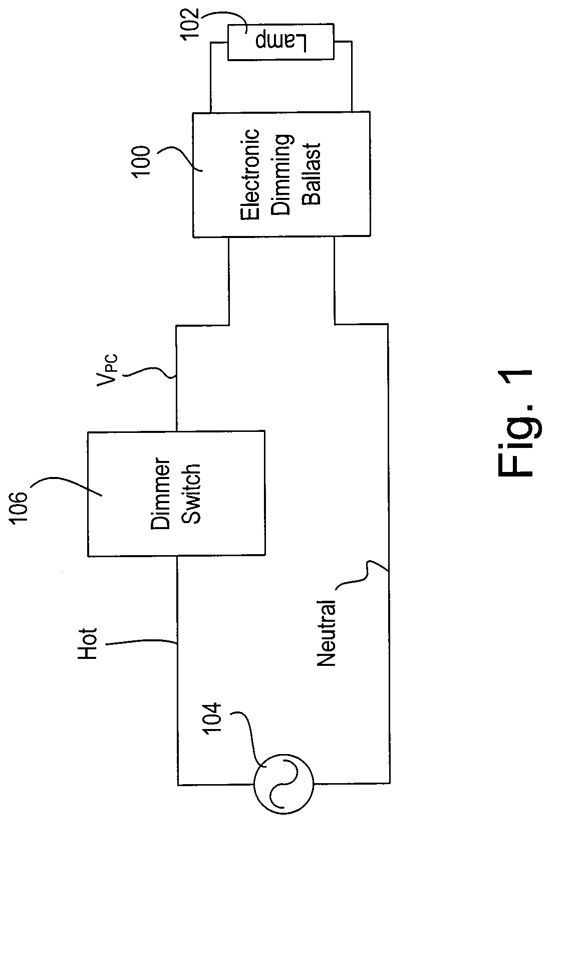
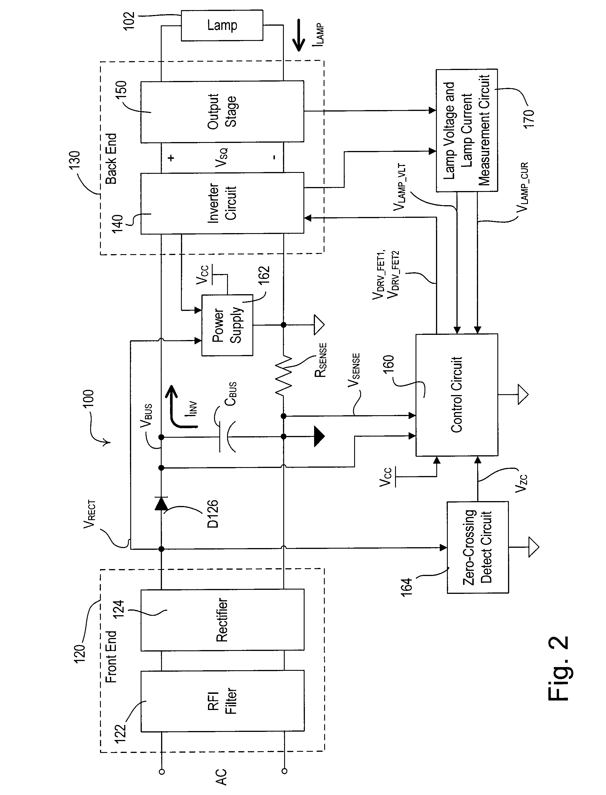
[0031]FIG. 1 is a simplified block diagram of a system including an electronic dimming ballast 100 for driving a fluorescent lamp 102 according to the present invention. The ballast 100 is coupled to the hot side of an alternating-current (AC) power source 104 (e.g., 120 VAC, 60 Hz) through a conventional two-wire dimmer switch 106. The dimmer switch 106 typically includes a bidirectional semiconductor switch (not shown), such as, for example, a triac or two field-effect transistors (FETs) coupled in anti-series connection, for providing a phase-controlled voltage VPC (i.e., a dimmed-hot voltage) to the ballast 100. Using a standard forward phase-control dimming technique, the bidirectional semiconductor switch is rendered conductive at a specific time each half-cycle of the AC power source and remains conductive for a conduction period TCON during each half-cycle. The dimmer switch 106 is operable to control the amount of power delivered to the ballast 100 by controlling the length...
second embodiment
[0104]FIG. 13 is a simplified block diagram of an electronic dimming ballast 1000 according to the present invention. The electronic dimming ballast 1000 comprises a charge pump circuit 1010, which is coupled in parallel electrical connection the diode D126 between the rectifier 124 and the inverter circuit 140. When the magnitude of the rectified voltage VRECT is less than the magnitude of the bus voltage VBUS, the charge pump circuit 1010 operates to draw a charge current ICP from the AC power source 104. Specifically, the charge pump circuit 1010 is coupled to the output of the inverter circuit 140, such that the charge pump circuit 1010 is operable to draw the charge current ICP every other half-cycle of the square-wave voltage VSQ. The charge current ICP drawn during the times that the magnitude of the rectified voltage VRECT is less than the magnitude of the bus voltage VBUS helps to prevent the current through the triac of the dimmer switch 106 from dropping below the holding...
third embodiment
[0108]FIG. 15 is a simplified schematic diagram of a lamp current measurement circuit 420′ of the measurement circuit 170 according to the present invention. A current transformer 270′ has two primary winding coupled between the resonant tank circuit 150 and to the lamp 102 as shown in FIG. 4. However, the current transformer 270′ only has a single secondary winding coupled to the lamp current measurement circuit 420′. Specifically, the secondary winding of the current transformer 270′ is coupled across the base-emitter junction of a PNP bipolar junction transistor Q1510. The junction of the base of the transistor Q1510 and the secondary winding of the current transformer 270′ is coupled to the DC supply voltage VCC. When the lamp current ILAMP (and thus the current through the secondary winding of the current transformer 270′) has a positive magnitude, the transistor Q1510 is rendered conductive, thus conducting current through a capacitor C1512 and a resistor R1514. The lamp curre...
PUM
 Abstract
Description
Claims
Application Information
 - R&D
- Intellectual Property
- Life Sciences
- Materials
- Tech Scout
- Unparalleled Data Quality
- Higher Quality Content
- 60% Fewer Hallucinations
Browse by: Latest US Patents, China's latest patents, Technical Efficacy Thesaurus, Application Domain, Technology Topic, Popular Technical Reports.
© 2025 PatSnap. All rights reserved.Legal|Privacy policy|Modern Slavery Act Transparency Statement|Sitemap|About US| Contact US: help@patsnap.com


