Electron source and image display apparatus
a technology of image display and electron source, which is applied in the direction of discharge tube/lamp details, discharge path lamps, discharge tubes luminescnet screens, etc., can solve the problem of device losing the electron emitting function, and achieve the effect of small variation in electron emission characteristi
- Summary
- Abstract
- Description
- Claims
- Application Information
AI Technical Summary
Benefits of technology
Problems solved by technology
Method used
Image

Examples
first embodiment
[0035](Configuration)
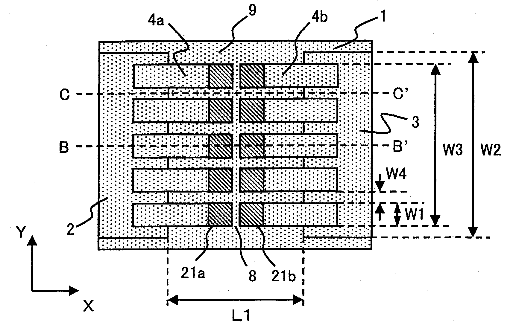
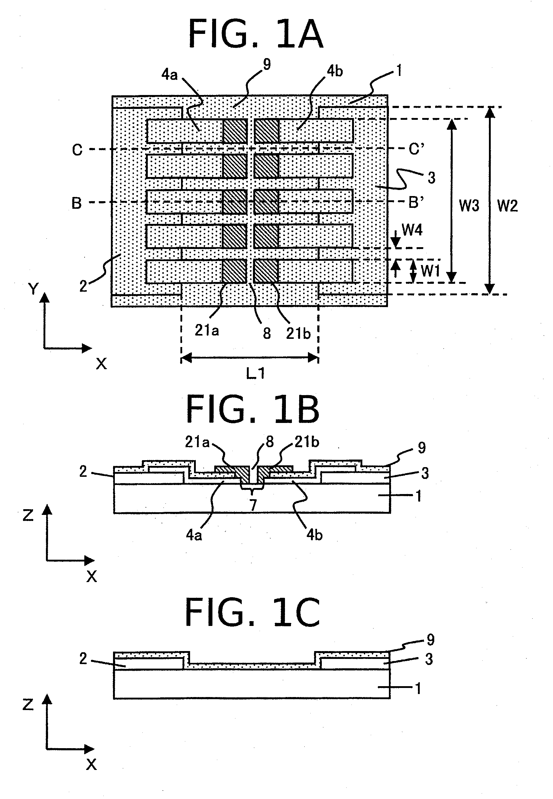
[0036]A configuration of the electron-emitting device according to the first embodiment is described with reference to FIGS. 1A to 1C. FIG. 1A is a plan view schematically illustrating a configuration of the electron-emitting device according to the first embodiment. FIGS. 1B and 1C are cross-sectional views taken along lines B-B′ and C-C′ of FIG. 1A, respectively.
[0037]As shown in FIGS. 1A to 1C, a pair of electrodes 2 and 3 is arranged on a substrate 1 so as to be separated from each other by a gap L1. A plurality of conductive films is provided between the pair of electrodes 2 and 3 on the substrate 1. The plurality of conductive films is electrically connected to the pair of electrodes, and has an electron emitting portion, respectively. Specifically, the conductive film having the electron emitting portion is separated into a conductive film 4a and a conductive film 4b by a first gap 7. The conductive film 4a connects the electrode 2 and a carbon film 21a, ...
second embodiment
[0081](Configuration)
[0082]A configuration of the electron-emitting device according to a second embodiment is described below with reference to FIGS. 6A to 6C. FIG. 6A is a plan view schematically illustrating the electron-emitting device according to the second embodiment. FIGS. 6B and 6C are cross-sectional views taken along lines B-B′ and C-C′ of FIG. 6A, respectively. In FIGS. 6A to 6C, the members which are the same as those described in the first embodiment are denoted by the same numbers. Further, since the size of L1, materials and sizes of the respective members in the electron-emitting device according to the second embodiment are similar to those described in the first embodiment, the description thereof will not be repeated.
[0083]The second embodiment is an example where an opposing direction of the carbon films 21a and 21b has an angle (preferably perpendicular) with respect to the substrate surface. Specifically, in the second embodiment, a side surface of a laminator...
example 1
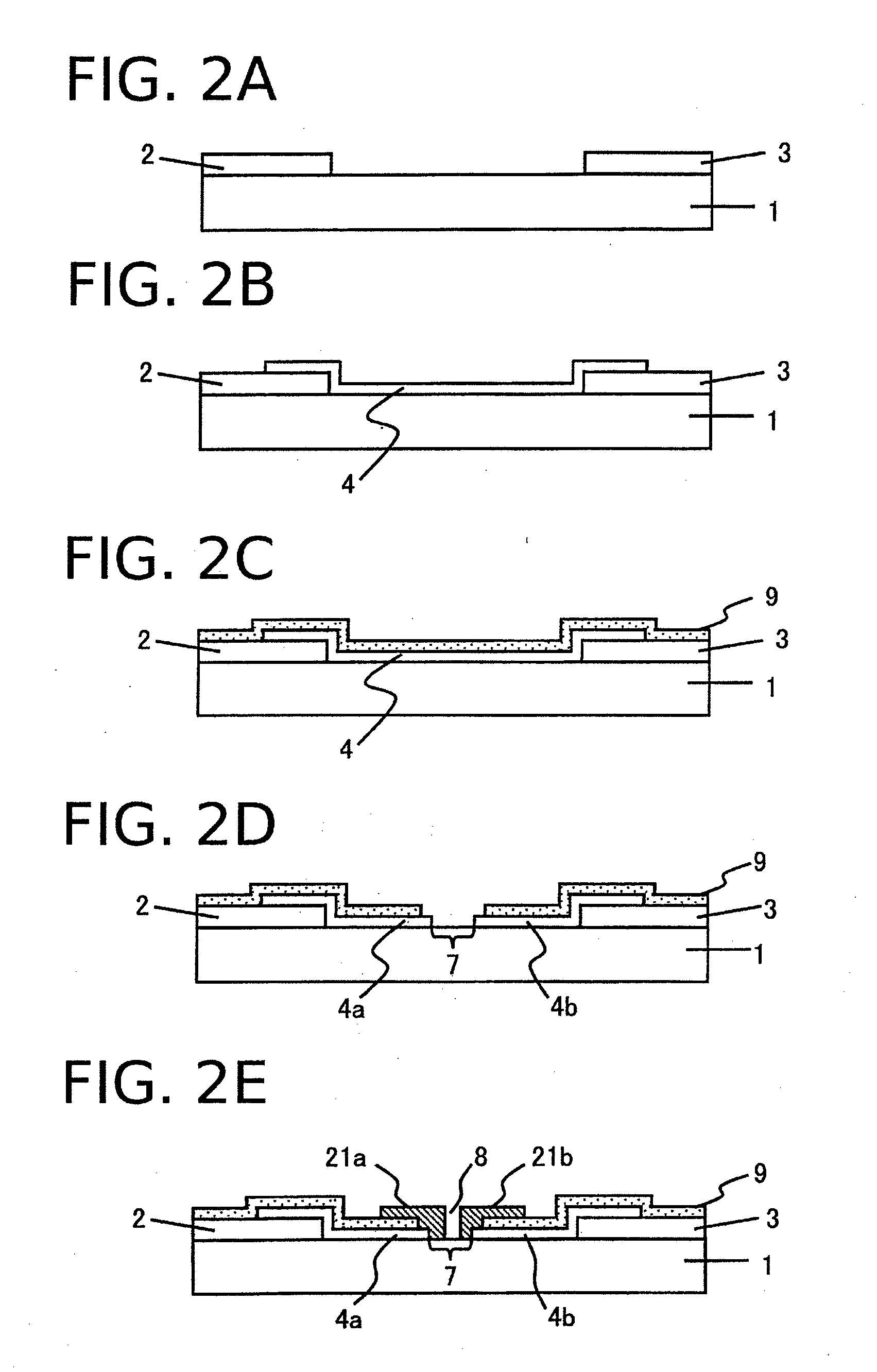
[0122]As an example 1, a concrete example of the electron-emitting device described in the first embodiment is described with reference to FIGS. 2A to 2E.
[0123](Step 1)
[0124]A quartz substrate for the substrate 1 is sufficiently rinsed. Ti with thickness of 5 nm is formed on the quartz substrate by the sputtering method, and Pt with thickness of 40 nm is formed on Ti. Thereafter, Ti and Pt are patterned into a desired shape by using the photolithography technique, so that Ti and Pt layers are formed as the electrodes 2 and 3 on the substrate 1 (FIG. 2A). At this time, the gap L1 between the electrodes 2 and 3 is set to 100 μm, and the width W2 of the electrodes 2 and 3 is set to 500 μm.
[0125](Step 2)
[0126]An organic palladium compound solution is spin-coated between the pair of electrodes 2 and 3 formed on the substrate 1 so as to be connected to the pair of the electrodes. Thereafter, the organic palladium compound solution is subject to the heating and baking process. Specifically...
PUM
 Abstract
Description
Claims
Application Information
 - R&D
- Intellectual Property
- Life Sciences
- Materials
- Tech Scout
- Unparalleled Data Quality
- Higher Quality Content
- 60% Fewer Hallucinations
Browse by: Latest US Patents, China's latest patents, Technical Efficacy Thesaurus, Application Domain, Technology Topic, Popular Technical Reports.
© 2025 PatSnap. All rights reserved.Legal|Privacy policy|Modern Slavery Act Transparency Statement|Sitemap|About US| Contact US: help@patsnap.com