Dynamic Reconfigurable Optical Interconnect System

a dynamic reconfigurable, optical interconnect technology, applied in the field of optics, can solve the problems of inflexible architecture for optical routing and chip-to-chip communication, and achieve the effect of reducing or eliminating at least some of the disadvantages and problems

Inactive Publication Date: 2010-03-04
FUJITSU LTD
View PDF14 Cites 5 Cited by
  • Summary
  • Abstract
  • Description
  • Claims
  • Application Information

AI Technical Summary

Benefits of technology

[0004]The present disclosure provides a dynamic reconfigurable optical interconnect system that substantially eliminates or reduces at least some of the disadvantages and problems associated with previous methods and systems.
[0006]Technical advantages of certain embodiments may include a reduction in wiring density requirements for a circuit board, a decrease in the number of active elements required to interconnect optical ports on a circuit board, a reduction in the cost of the overall system, and / or an increase in overall system performance. Other advantages may include higher flexibility for optical signal routing, a reduction in the crosstalk between optical channels, and an increase in system bandwidth. Embodiments may eliminate certain inefficiencies such as requiring a dedicated optical channel waveguide between every optical data port on a circuit board. Some embodiments may also eliminate the need for additional multiplexing devices in order to provide wavelength multiplexing capabilities.

Problems solved by technology

This results in an inflexible architecture for optical routing and chip-to-chip communication.

Method used


Image

  • Dynamic Reconfigurable Optical Interconnect System
  • Dynamic Reconfigurable Optical Interconnect System
  • Dynamic Reconfigurable Optical Interconnect System

Examples


Embodiment Construction

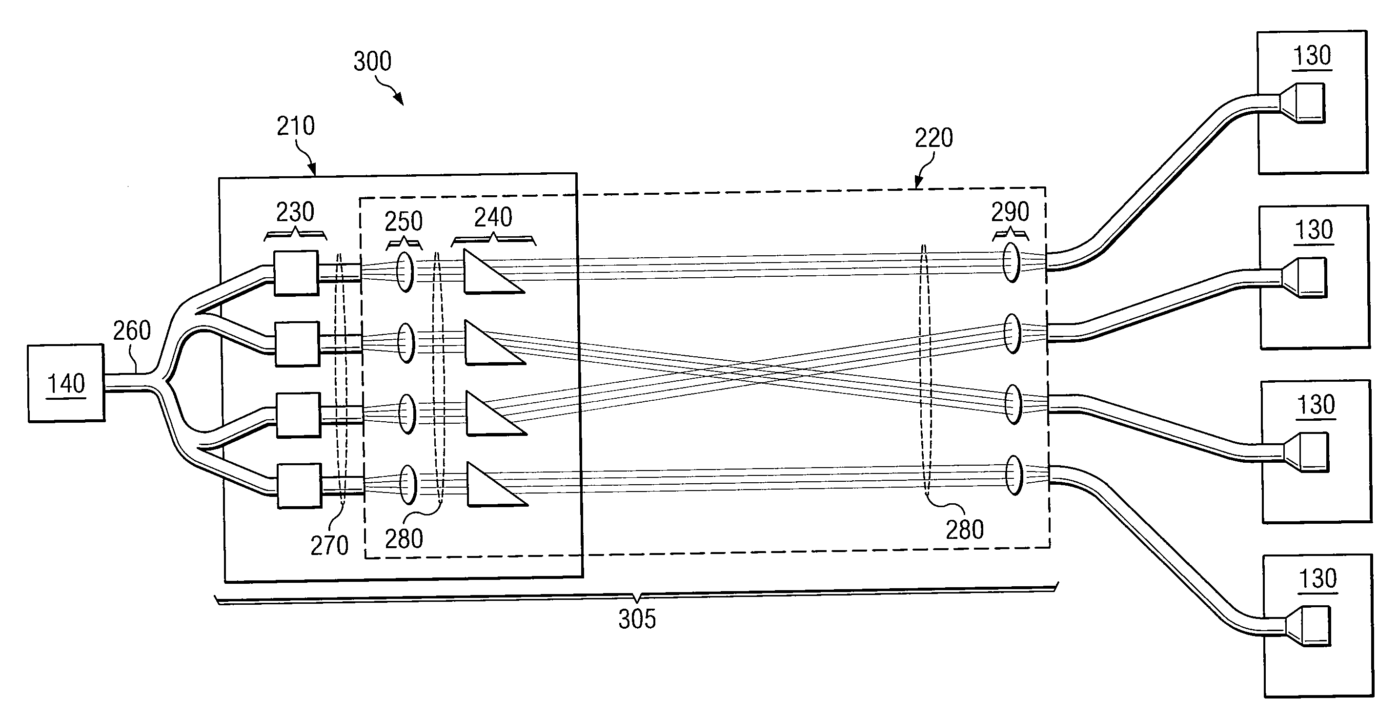
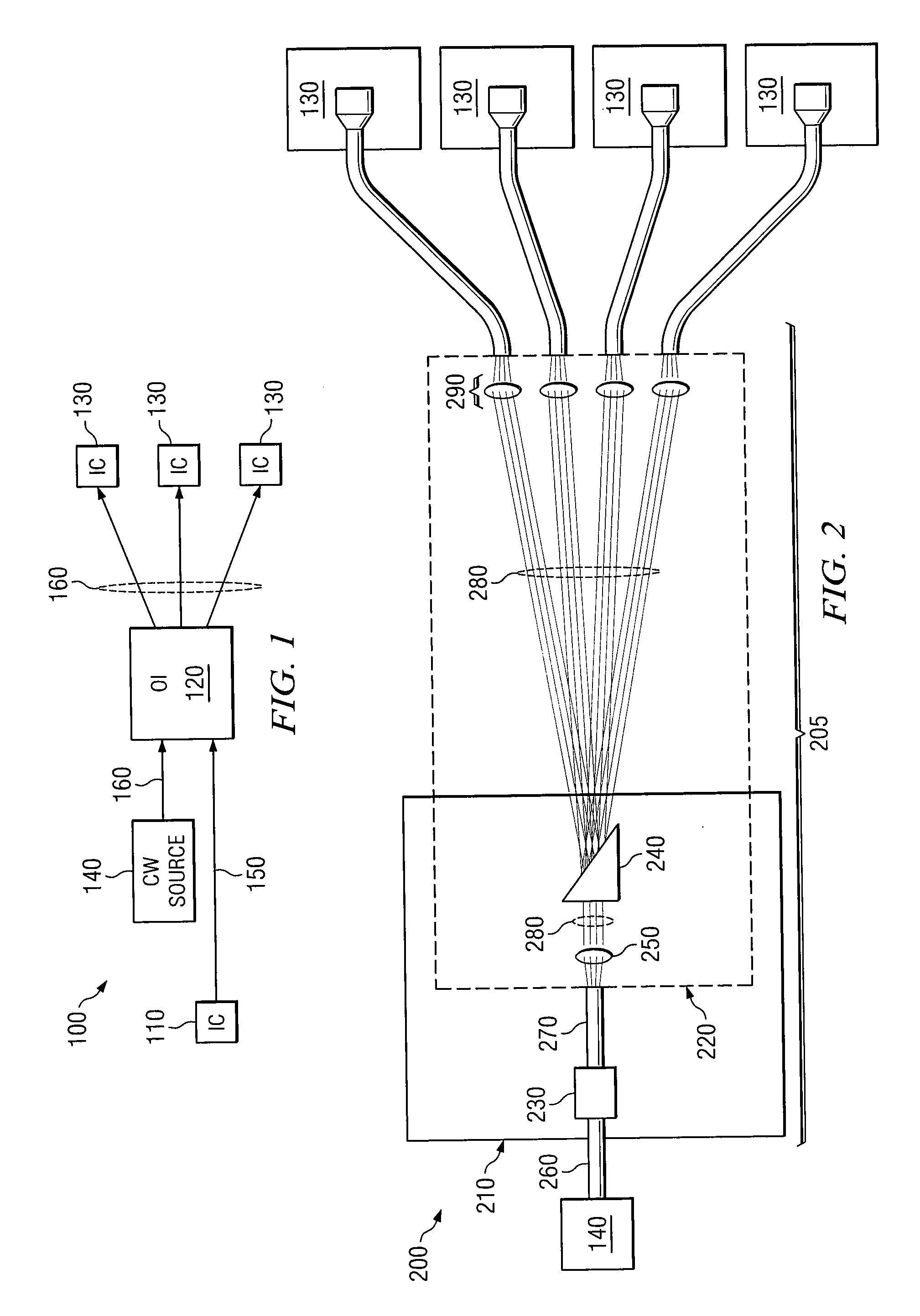
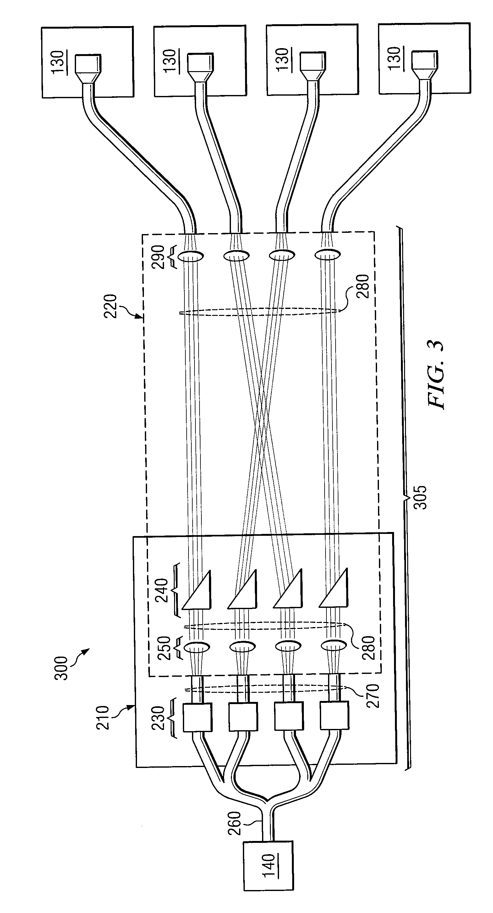
[0013]FIG. 1 depicts an optical circuit 100 where a particular embodiment may be utilized. Optical circuit 100 includes a data source 110, an optical interconnect 120, one or more receiving devices 130, and a continuous wave (“CW”) light source 140. Data source 110 is coupled to optical interconnect 120 via an electrical data link 150. CW light source 140 is coupled to optical interconnect 120 via an optical link 160. Optical interconnect 120 is also coupled to receiving devices 130 via optical links 160. Optical links 160 include, but are not limited to, optical waveguides, such as rectangular waveguides, slab waveguides, optical fibers, and the like. Data source 110 and receiving devices 130 may be integrated circuits (“IC”), or any other suitable device that transmits and / or receives data.

[0014]In operation, data source 110 outputs data to optical interconnect 120 via electrical data link 150. Optical interconnect 120 receives this data, along with a CW light beam from CW light s...


PUM

PropertyMeasurementUnit
input voltageaaaaaaaaaa
refractive indexaaaaaaaaaa
wavelengthaaaaaaaaaa

Abstract

An optical interconnect system includes an integrated circuit, at least one optical modulator, and a slab waveguide. The optical modulator is coupled to the integrated circuit and receives an input light beam from a light source and data from a source device and generates a modulated output light beam. The slab waveguide is coupled to the optical modulator and includes at least one input waveguide microlens, a plurality of output waveguide microlenses, and at least one deflector prism. The input waveguide microlens focuses the modulated output light beam from the modulator into a collimated light beam. The deflector prism is coupled to the integrated circuit, receives the collimated light beam from the input waveguide microlens, and deflects the collimated light beam toward one of the output waveguide microlenses according to an input voltage.

Description

TECHNICAL FIELD[0001]This disclosure relates in general to optics and more particularly to a dynamic reconfigurable optical interconnect system.BACKGROUND[0002]Optical interconnects are likely replacements for traditional electrical interconnects between components on circuit boards. Unlike electrical interconnects, optical interconnects provide little or no signal propagation delay. In addition, optical interconnects provide for a significant increase to the available bandwidth of board-level interconnects.[0003]Traditional optical interconnects employ predefined optical paths between data ports on various components. These paths typically consist of fixed optical channel waveguides that are formed on a substrate. These paths are dedicated paths that may only be utilized by the two data ports to which they connect. This results in an inflexible architecture for optical routing and chip-to-chip communication.SUMMARY OF THE DISCLOSURE[0004]The present disclosure provides a dynamic re...

Claims


Application Information

Patent Timeline
Patent Type & Authority Applications(United States)
IPC IPC(8): G02B6/12G02F1/295
CPCG02B6/3524G02B6/3528G02B6/3546H04Q2011/003G02F1/295H04J14/02H04Q11/0005G02B6/356
Inventor GLEBOV, ALEXEI L.LEE, MICHAEL G.
Owner FUJITSU LTD
Why Eureka
Try Eureka