
Branching filter, semiconductor integrated circuit device, and communication mobile terminal

Active Publication Date: 2010-03-04
MURATA MFG CO LTD
View PDF8 Cites 14 Cited by
  • Summary
  • Abstract
  • Description
  • Claims
  • Application Information

AI Technical Summary

Benefits of technology

[0027]Enumerated below are advantageous effects to be provided according to the representative aspects of the present invention:
to be provided according to the representative aspects of the present invention:
(1) In a branching filter, the anti-ESD characteristic and harmonic attenuation characteristic thereof can be enhanced while reducing the circuit size thereof.
(2) Based on the above advantageous effect (1), it is possible to reduce the size of a high-frequency power amplifier module and increase the performance capabilities thereof while realizing reduction in cost.
(3) Based on the above advantageous effects (1) and (2), a communication mobile terminal having higher functional performance can be provided at lower cost.

Problems solved by technology

However, since the pHEMT switch is vulnerable to electrostatic breakdown, it is required to improve anti-ESD characteristic particularly in a low frequency band circuit where the passing-through of an ESD signal is likely to occur.

Method used


Image

  • Branching filter, semiconductor integrated circuit device, and communication mobile terminal
  • Branching filter, semiconductor integrated circuit device, and communication mobile terminal
  • Branching filter, semiconductor integrated circuit device, and communication mobile terminal

Examples


embodiment 1

Preferred Embodiment 1

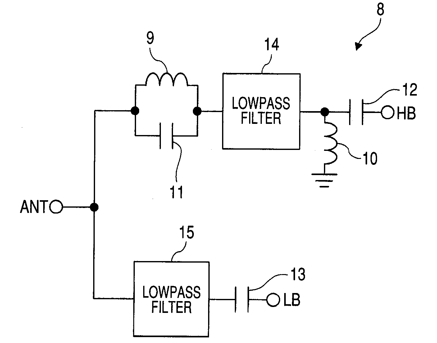
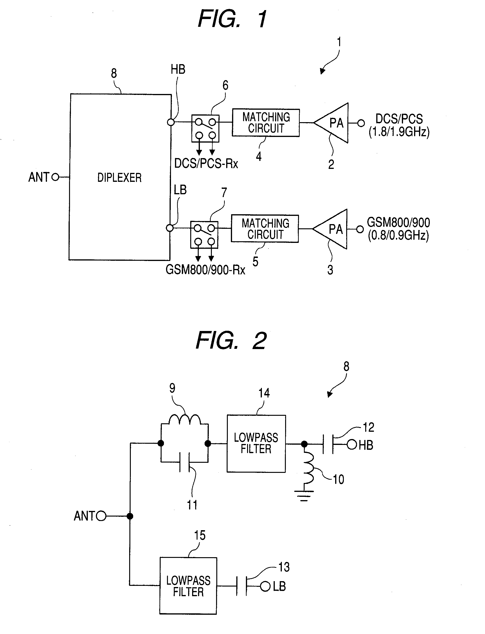
[0042]FIG. 1 shows a block diagram of an exemplary configuration of a high-frequency power amplifier module according to a preferred embodiment 1 of the present invention, and FIG. 2 shows an explanatory diagram of an exemplary configuration of a diplexer included in the high-frequency power amplifier module illustrated in FIG. 1.

[0043]In the present preferred embodiment 1, a high-frequency power amplifier module 1 is a transmission power amplifier module contained in a mobile phone (communication mobile terminal) to be used in a communication system, for example. The high-frequency power amplifier module 1, which is provided in the form of a semiconductor integrated circuit device, comprises output power amplifiers 2 and 3, matching circuits 4 and 5, antenna switch circuits 6 and 7, a diplexer 8, etc.

[0044]The output power amplifier 2 is used to amplify transmitting signals in a high frequency band (e.g., DCS / PCS (1.8 GHz band / 1.9 GHz band)). The output power ...

embodiment 2

Preferred Embodiment 2

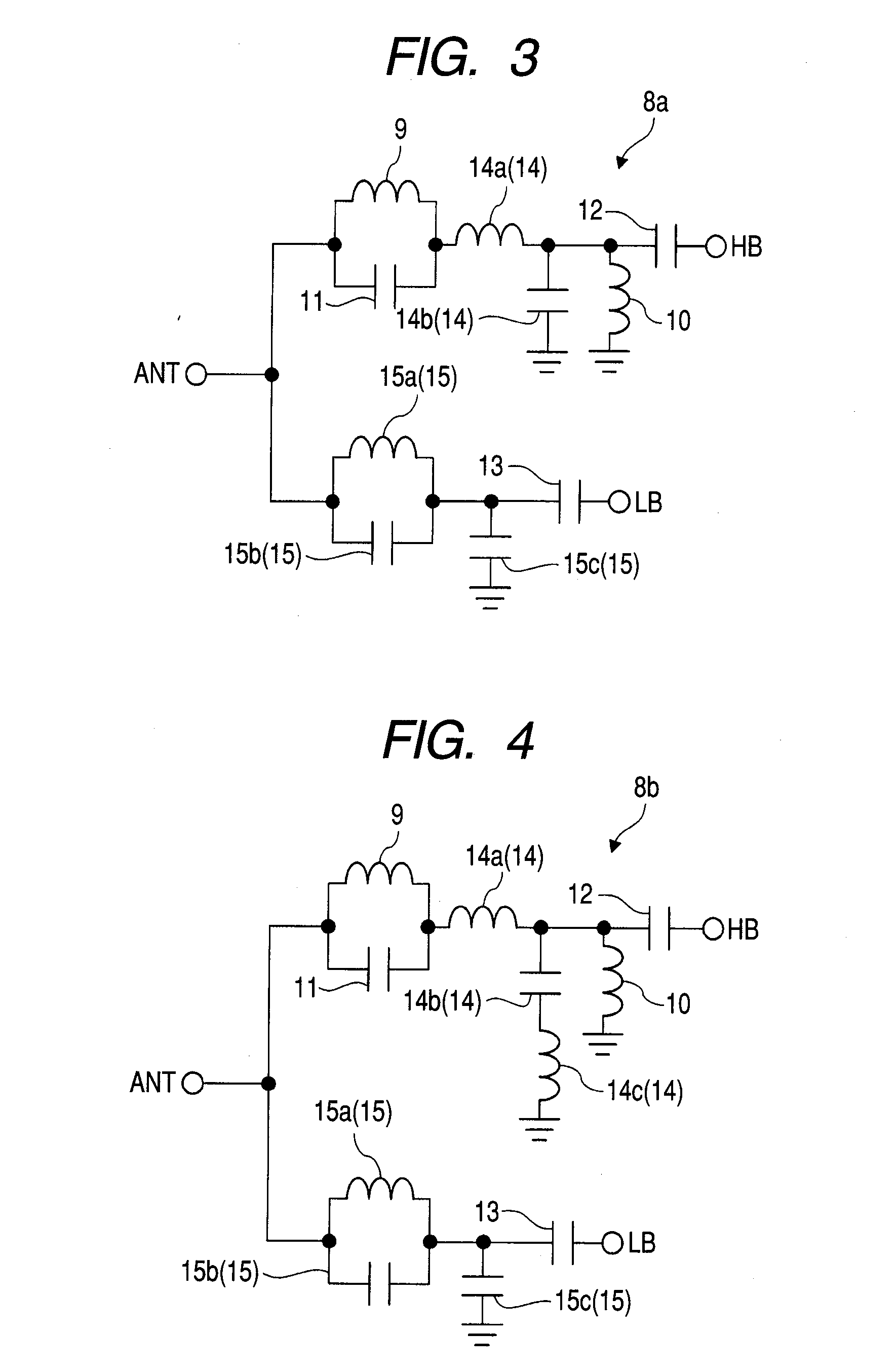
[0065]Referring to FIG. 3, there is shown an exemplary configuration of a diplexer according to a preferred embodiment 2 of the present invention.

[0066]In the present preferred embodiment 2, the high-frequency power amplifier module 1 comprises output power amplifiers 2 and 3, matching circuits 4 and 5, antenna switch circuits 6 and 7, a diplexer 8a, etc. in a fashion similar to that in the preferred embodiment 1 (FIG. 1) demonstrated above.

[0067]As shown in FIG. 3, the diplexer 8a comprises inductors 9 and 10, electrostatic capacitor elements 11 to 13, and lowpass filters 14 and 15. The lowpass filter 14 comprises an inductor 14a serving as a first filter-circuit inductor and an electrostatic capacitor element 14b serving as a first filter-circuit electrostatic capacitor element, and the lowpass filter 15 comprises an inductor 15a and electrostatic capacitor elements 15b and 15c. Further, a second tank circuit is formed of the inductor 15a and the electrostati...

embodiment 3

Preferred Embodiment 3

[0076]FIG. 4 shows an explanatory diagram of an exemplary configuration of a diplexer according to a preferred embodiment 3 of the present invention, and FIG. 5 shows an explanatory diagram of an exemplary frequency characteristic of the diplexer illustrated in FIG. 4.

[0077]In the present preferred embodiment 3, the high-frequency power amplifier module 1 comprises output power amplifiers 2 and 3, matching circuits 4 and 5, antenna switch circuits 6 and 7, a diplexer 8b, etc. in a fashion similar to that in the foregoing preferred embodiment 1 (FIG. 1).

[0078]As shown in FIG. 4, the diplexer 8b comprises inductors 9 and 10, electrostatic capacitor elements 11 to 13, and lowpass filters 14 and 15. In comparison with the preferred embodiment 2 (FIG. 3) demonstrated above in which the lowpass filter 14 comprises an inductor 14a and an electrostatic capacitor element 14b, the lowpass filter 14 in the present preferred embodiment 3 further comprises an inductor 14c s...


PUM


Abstract

A technique for realizing module size reduction while enhancing the anti-ESD characteristic of a low frequency band circuit without the need to add such an element as an ESD filter. In a diplexer included in a high-frequency power amplifier module, a composite grounding inductor with respect to an antenna terminal is formed of three inductors including a series inductor contained in a lowpass filter. Since an ESD signal contains main components thereof belonging to a frequency band of the order of a few hundreds of MHz or lower, the ESD signal is allowed to pass through a lowpass filter almost intactly. Under this condition, a function for ESD filtering from the antenna terminal to an antenna switch circuit is provided by using the composite grounding inductor mentioned above and an electrostatic capacitor element, thereby suppressing passage of the ESD signal to the antenna switch circuit.

Description

CROSS-REFERENCE TO RELATED APPLICATIONS[0001]The disclosure of Japanese Patent Application No. 2008-218050 filed on Aug. 27, 2008 including the specification, drawings and abstract is incorporated herein by reference in its entirety.BACKGROUND OF THE INVENTION[0002]The present invention relates to a technique for enhancing the performance of a high-frequency power amplifier module used in a communication mobile terminal or the like, and more particularly to a technique effectively applicable to anti-ESD (ElectroStatic Discharge) characteristic enhancement and harmonic suppression in a branching filter of the high-frequency power amplifier module.[0003]Recent years have seen the widespread proliferation of mobile phones used as terminal units for mobile telecommunication, and at present, there is an increasing demand for implementation of more diverse functionalities in mobile phones. Regarding a high-frequency power amplifier module contained in a mobile phone for example, it is des...

Claims


Application Information

Patent Timeline
IPC IPC(8): H03H7/01H03H7/075H03H7/46H04B1/3822H04B1/40
CPCH03H7/463H03H7/175H03H7/1758H03H7/1791H03H7/1775H03H7/1783H03H7/1766
Inventor OKABE, HIROSHI
Owner MURATA MFG CO LTD
Learn More