
Transistor structure and dynamic random access memory structure including the same

a technology of dynamic random access and transistor, applied in the direction of transistor, semiconductor device, electrical apparatus, etc., can solve the problems of inferior performance of transistors such as obtained, and the sgt also faces the challenge of floating body effect, so as to achieve better properties

Active Publication Date: 2010-03-04
NAN YA TECH
View PDF4 Cites 93 Cited by
  • Summary
  • Abstract
  • Description
  • Claims
  • Application Information

AI Technical Summary

Benefits of technology

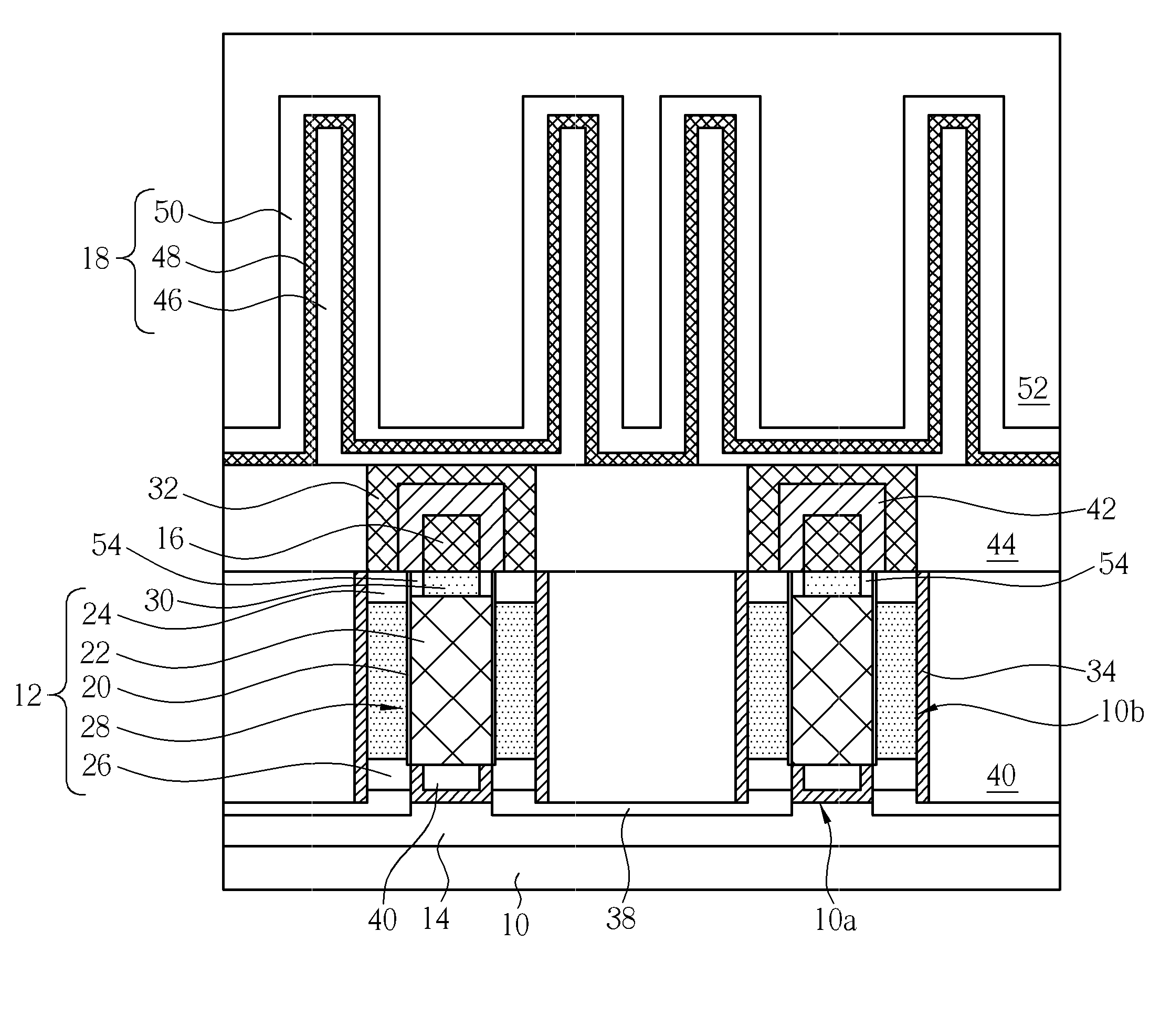
[0010]In comparison with the conventional techniques, in the DRAM structure of the present invention, the SGT is formed on the substrate inside the donut-type pillar and the donut-type pillar is used to serve as a gate channel. There are many advantages that it is suitable for mass production since the donut-type pillar can be defined directly by bulk silicon etching; the gate channel can be formed of single crystal silicon with better properties; and the gate structures can be easily combined with the capacitor through a node contact having a distinct structure.

Problems solved by technology

However, the epitaxial silicon is often inferior in properties to the bulk silicon, such that transistors such obtained tend to be inferior in performance.
The SGT also faces a challenge of floating body effect due to the source / drain placed at the top / bottom of the channel.

Method used


Image

  • Transistor structure and dynamic random access memory structure including the same
  • Transistor structure and dynamic random access memory structure including the same
  • Transistor structure and dynamic random access memory structure including the same

Examples


Embodiment Construction

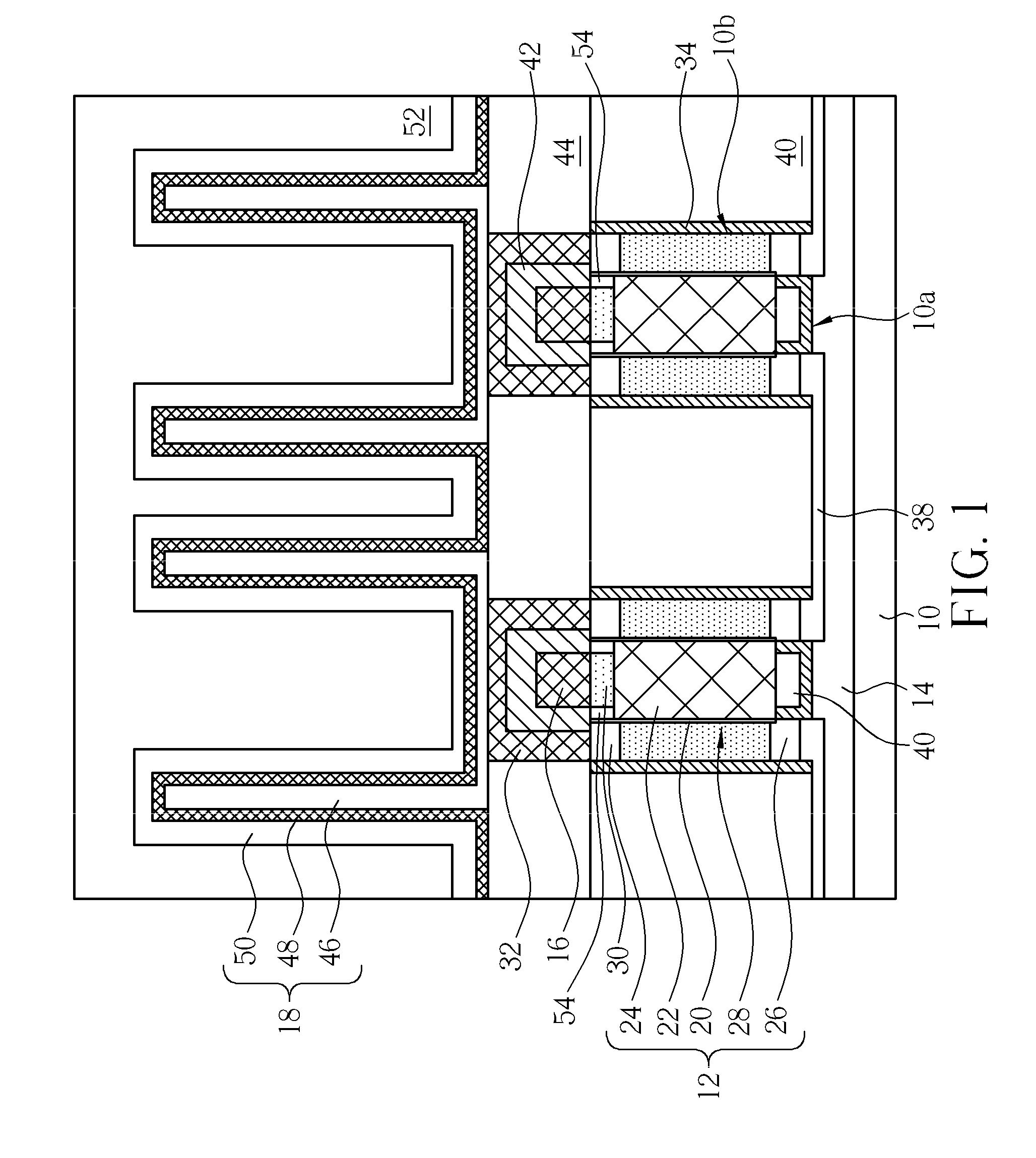
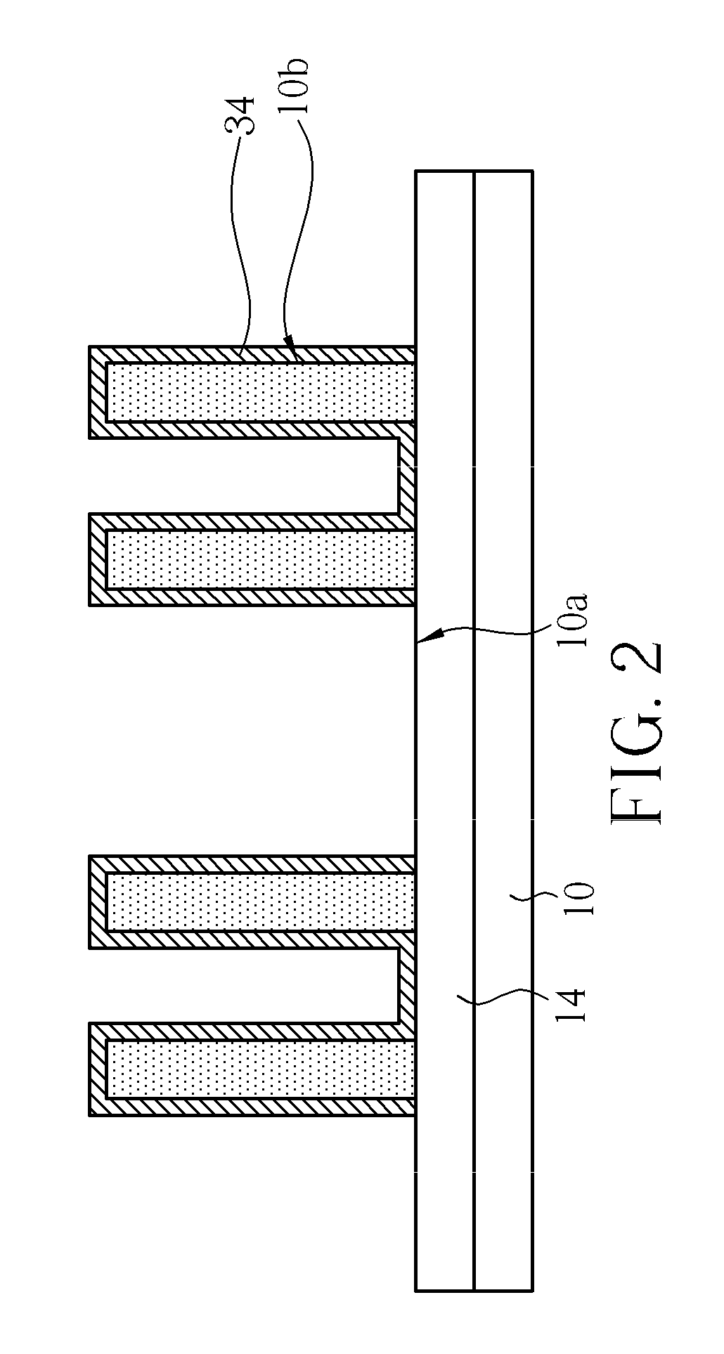
[0016]Referring to FIG. 1, the DRAM structure according to the present invention includes a substrate 10, a transistor 12, a bit line 14, a word line 16, and a capacitor 18. The substrate 10 has a plane 10a and a donut-type pillar 10b extending upward from the plane 10a of the substrate 10. The donut-type pillar 10b serves as an active area. The donut-type pillar 10b is in an annular shape, and therefore it has an outer wall at the perimeter of the pillar, a central cavity defined in a central portion of the outer wall, and an inner wall surrounding the central cavity.

[0017]The annular shape herein may be round, square, or in other shape. The thickness of the annular wall is not particularly limited and may be preferably for example 100 Å to 3000 Å, and more preferably 500 Å to 2000 Å, depending on the process technology and the device properties. The transistor 12 is disposed inside the donut-type pillar 10b and includes a gate dielectric layer 20, a gate 22, an upper source / drain ...


PUM


Abstract

A dynamic random access memory structure is disclosed, in which, the active area is a donut-type pillar at which a novel vertical transistor is disposed and has a gate filled in the central cavity of the pillar and upper and lower sources / drains located in the upper and the lower portions of the pillar respectively. A buried bit line is formed in the substrate beneath the transistor. A word line is horizontally disposed above the gate. A capacitor is disposed above the word line as well as the gate and electrically connected to the upper source / drain through a node contact. The node contact has a reverse-trench shape with the top surface electrically connected to the capacitor and with the bottom of the sidewalls electrically connected to the upper source / drain. The word line passes through the space confined by the reverse-trench shape.

Description

BACKGROUND OF THE INVENTION[0001]1. Field of the Invention[0002]The present invention relates to a vertical transistor and a dynamic random access memory (DRAM) structure including therein the vertical transistor.[0003]2. Description of the Prior Art[0004]Along with the miniaturization of various electronic products, the dynamic random access memory (DRAM) elements have to meet the demand of high integration and high density. A DRAM structure includes a capacitor for holding a charge and a transistor for accessing the charge held in the capacitor. DRAMs with trench capacitors or stacked capacitors are widely used in the industry so as to well utilize space of chips to effectively reduce memory cell size. Typically, trench capacitors are fabricated inside deep trenches that are formed in a semiconductor substrate by an etching process, followed by the manufacturing process of transistors. Stacked capacitors are generally formed after formation of transistors, and located on the trans...

Claims


Application Information

Patent Timeline
Patent Type & Authority Applications(United States)
IPC IPC(8): H01L27/108H10B12/00
CPCH01L27/10876H01L29/7827H01L29/66666H10B12/053
Inventor HUANG, WEN-KUEI
Owner NAN YA TECH
Learn More