Sputtering deposition apparatus and backing plate for use in sputtering deposition apparatus
- Summary
- Abstract
- Description
- Claims
- Application Information
AI Technical Summary
Benefits of technology
Problems solved by technology
Method used
Image

Examples
example
Example 1
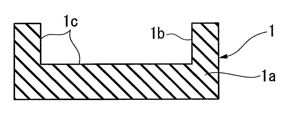
[0113]A backing plate made of a polysilicon as shown in FIG. 1 was produced by molding a base material made of a polysilicon.
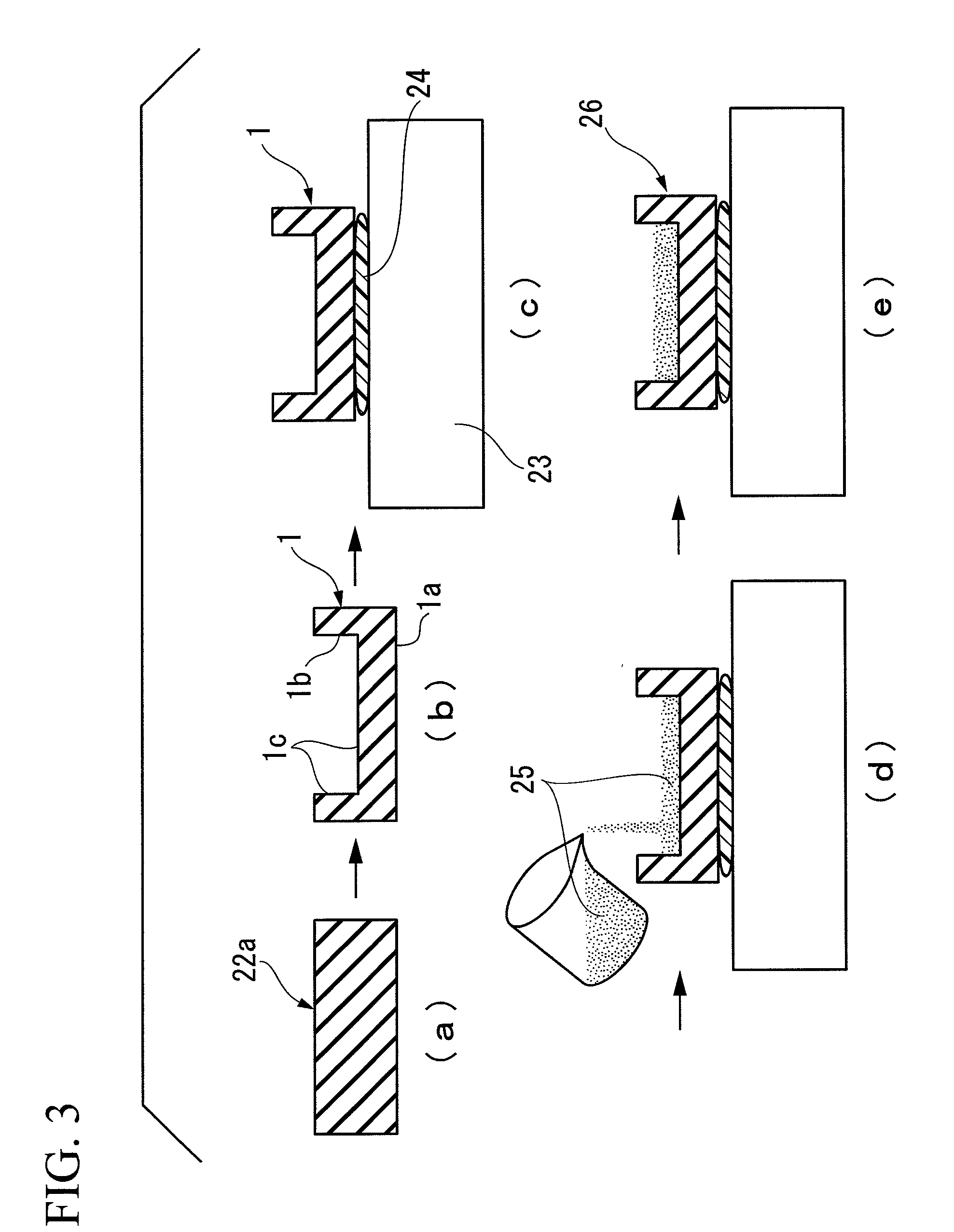
[0114]Next, after the above backing plate was soaked into an organic solvent such as IPA to be cleaned, the resultant backing plate was fixed to a cooling plate using an adhesive. Several Ga particles were put into a beaker, heated at 60° C. to melt them into a liquid, and thereafter the resultant liquid Ga was poured into the reentrant of the backing plate, and then cooled to a room temperature 25° C. at which clean room was set to solidify Ga, thereby producing a sputter target.
[0115]In addition, as shown in FIG. 5, this sputter target was installed to a predetermined position in a chamber of a sputter deposition apparatus, and a sapphire substrate was installed on an upper part thereof. In the sputter deposition apparatus, the sapphire substrate was heated to 500° C., nitrogen gas was introduced thereinto at a flow rate of 15 sccm, the pressure in ...
example 2
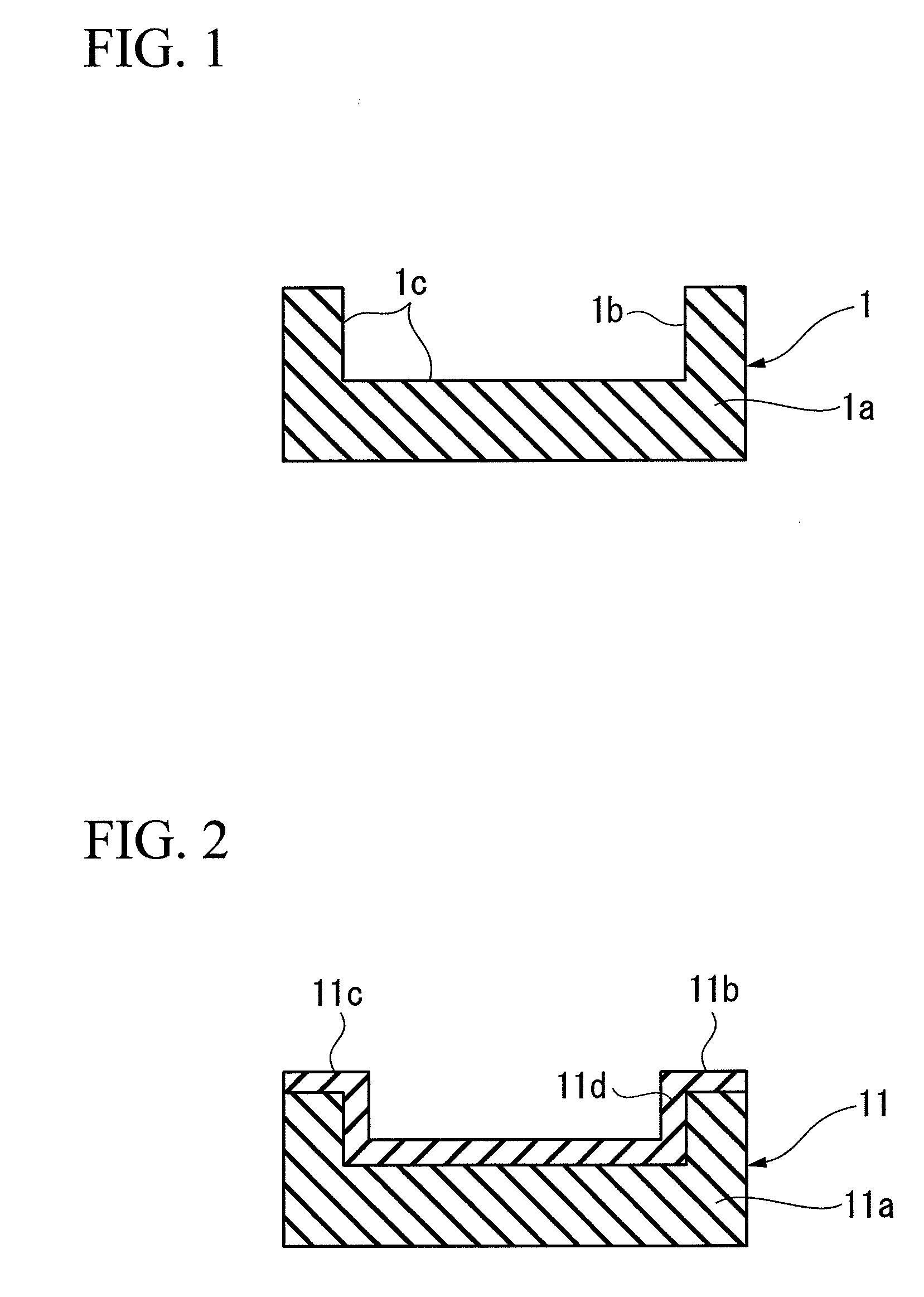
[0116]A base material made of Cu was molded, and a carbon coating was performed by CVD method to produce a backing plate, as shown in FIG. 2, which is made of Cu and coated with carbon having a thickness of 200 μm.
[0117]Next, a sputter target was produced similarly to Example 1. In addition, the sputter target was cooled by a cooling plate, and a single layer film of Ga N was formed on a sapphire substrate by the same way as in Example 1 with the exception of sputtering Ga in a solid state.
[0118]The resultant single layer film of Ga N was taken out, and was subjected to SIMS analysis. As a result of examining whether Cu and C were detected as impurities, but it was lower than the detective level of SIMS.
example 3
[0119]A base material made by SiO2 is molded, and a backing plate made of SiO2 as shown in FIG. 1, was produced.
[0120]Next, after the above backing plate was soaked into an organic solvent such as IPA to be cleaned, the resultant backing plate was fixed to a cooling plate using an adhesive. Several Ga particles were put into a beaker, heated at 60° C. to melt them into a liquid, and thereafter Al wire rods having a diameter of approximately 1 mm cut into a length of 2 to 3 cm were added thereto at a percentage of 8 g of Al per 1 kg of Ga and melted, and the resultant molten material was poured into the reentrant of the backing plate, and then cooled to a room temperature 25° C. at which clean room was set to solidify Ga Al, thereby producing a sputter target.
[0121]In addition, a single layer film of AlGaN was formed on the sapphire substrate in the same way as in Example 1.
[0122]The resultant single layer film of AlGaN was taken out, and was subjected to SIMS analysis. Si concentrat...
PUM
| Property | Measurement | Unit |
|---|---|---|
| Contact angle | aaaaa | aaaaa |
| Semiconductor properties | aaaaa | aaaaa |
| Wettability | aaaaa | aaaaa |
Abstract
Description
Claims
Application Information
 - R&D
- Intellectual Property
- Life Sciences
- Materials
- Tech Scout
- Unparalleled Data Quality
- Higher Quality Content
- 60% Fewer Hallucinations
Browse by: Latest US Patents, China's latest patents, Technical Efficacy Thesaurus, Application Domain, Technology Topic, Popular Technical Reports.
© 2025 PatSnap. All rights reserved.Legal|Privacy policy|Modern Slavery Act Transparency Statement|Sitemap|About US| Contact US: help@patsnap.com