Resistance ram having oxide layer and solid electrolyte layer, and method for operating the same

Inactive Publication Date: 2010-01-07
GWANGJU INST OF SCI & TECH
View PDF27 Cites 24 Cited by
  • Summary
  • Abstract
  • Description
  • Claims
  • Application Information

AI Technical Summary

Benefits of technology

[0006]The present invention has been made keeping in mind the above problems occurring in the related arts, an object of the present invention is to provide a resistance RAM that can lower a resistor distribution.
[0013]According to the present invention, the resistance RAM that includes the oxide layer and the solid electrolyte layer as the resistance layer forms a conductive tip in the oxide layer by a foaming process, and may control the position and the number of conductive filaments that are formed in the solid electrolyte layer by concentrating an electric filed at the conductive tip in a reset step. Therefore, in the set step-reset step, that is, in the repeated switching operation between the low resistance state and the high resistance state, since the same conductive filament can be formed or removed, it is possible to ensure the uniform resistance switching characteristic.

Problems solved by technology

However, it is very difficult to control the formation position and the formation amount of the conductive channel.
Accordingly, when the element is switched repeatedly, since resistor distribution of each of the low resistance state and the high resistance state is very large, a nonuniform resistance switching characteristic may be shown, and because of the large resistor distribution of each of the two resistance states, it is difficult to discriminate the two resistance states.

Method used


Image

  • Resistance ram having oxide layer and solid electrolyte layer, and method for operating the same
  • Resistance ram having oxide layer and solid electrolyte layer, and method for operating the same
  • Resistance ram having oxide layer and solid electrolyte layer, and method for operating the same

Examples


preparation example

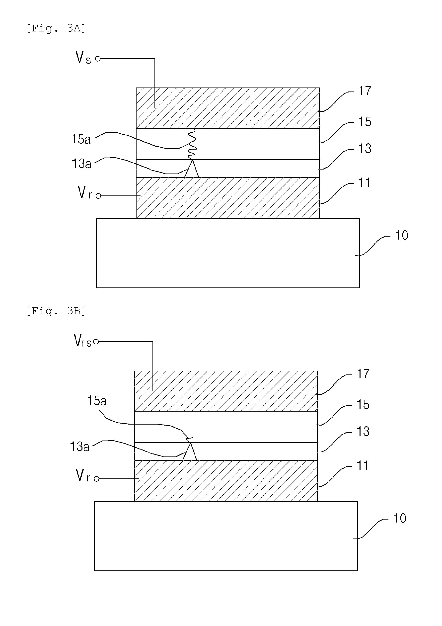
[0042]After the silicon oxide layer and the titanium layer are formed on the silicon substrate, the Pt layer is formed as the first electrode. On the Pt layer, the Gd2O3 layer as the oxide layer was formed in a thickness of 10 nm by using a deposition method. On the Gd2O3 layer, the MoOx layer (X:1.5-2.5) that is doped with Cu in an amount of 10 at. %, that is, the Cu:MoOx layer, as the solid electrolyte layer that is doped with the metal ion was formed in a thickness of 50 nm by using a deposition method. On the Cu:MoOx layer, the Pt layer as the second electrode was formed, such that the resistance RAM was prepared.


PUM


Abstract

A resistance RAM that is provided with an oxide layer and a solid electrolyte layer, and a method for operating the same are provided. The resistance RAM comprises a first electrode, an oxide layer that is formed on the first electrode, a solid electrolyte layer that is disposed on the oxide layer, and a second electrode that is disposed on the solid electrolyte layer. The method comprises the step of forming a conductive tip in the oxide layer by applying reference voltage to any one of the electrodes of the resistance RAM, applying foaming voltage to the remain one, such that the oxide layer is electrically broken. A conductive filament is formed in the solid electrolyte layer by applying a positive voltage to the second electrode on the basis of the voltage that is applied to the first electrode. The conductive filament that is formed in the solid electrolyte layer is removed by applying a negative voltage to the second electrode on the basis of the voltage that is applied to the first electrode.

Description

BACKGROUND OF THE INVENTION[0001]1. Field of the Invention[0002]The present invention relates to a nonvolatile RAM, and more particularly, to a resistance RAM.[0003]2. Description of the Related Art[0004]Currently, in the case of a flash memory that is commercialized with a nonvolatile memory, an electric charge is stored or removed in an electric charge storage layer, such that a change in threshold voltage is used. The electric charge storage layer may be a floating gate that is a polysilicon layer or an electric charge trap layer that is a silicon nitride layer. Recently, a novel nonvolatile RAM that has low power consumption and high degree of integration as compared to the flash RAM has been studied. As examples of the novel nonvolatile RAMs, there are a phase change RAM, a magnetic RAM and a resistance RAM.[0005]The resistance RAM may have a structure in which a solid electrolyte layer is inserted between metal electrodes. This element may generate or remove a conductive chann...

Claims


Application Information

Patent Timeline
IPC IPC(8): G11C11/00H01L47/00
CPCH01L45/085H01L45/146H01L45/143H01L45/1233H01L45/142H01L45/12H10N70/801H10N70/245H10N70/826H10N70/8822H10N70/8825H10N70/8833G11C13/0004
Inventor HWANG, HYUN SANGYOON, JAESIK
Owner GWANGJU INST OF SCI & TECH
Why Eureka
Try Eureka