Flip-chip light emitting diode and method for fabricating the same

Inactive Publication Date: 2009-12-31
ADVANCED OPTOELECTRONICS TECH
View PDF10 Cites 304 Cited by
  • Summary
  • Abstract
  • Description
  • Claims
  • Application Information

AI Technical Summary

Benefits of technology

[0004]A flip-chip semiconductor package refers to a package structure using a flip-chip technique to electrically connect an active surface of a chip to a surface of a structure via a plurality of conductive bumps. A plurality of solder balls are implanted on another surface of the substrate and serves as input / output (I / O) connections to allow the chip to be electrically connected to an external device. In the above arrangement, the size of the semiconductor package can be significantly reduced such that the chip may be made dimensionally closer to that of the substrate, and the semiconductor package does not require bonding wires, thereby reducing impedance and improving the electrical performance of the semiconductor package. These advantages make the flip-chip packaging technology become the mainstream packaging technology.

Problems solved by technology

However, the chip 63 tends to translocate with respect to the submounts 62 due to the bonding strength of the conductive bumps 64 and the submounts 62, resulting in a poor electrical connection between the chip 63 and the submounts 62.

Method used


Image

  • Flip-chip light emitting diode and method for fabricating the same
  • Flip-chip light emitting diode and method for fabricating the same
  • Flip-chip light emitting diode and method for fabricating the same

Examples


Embodiment Construction

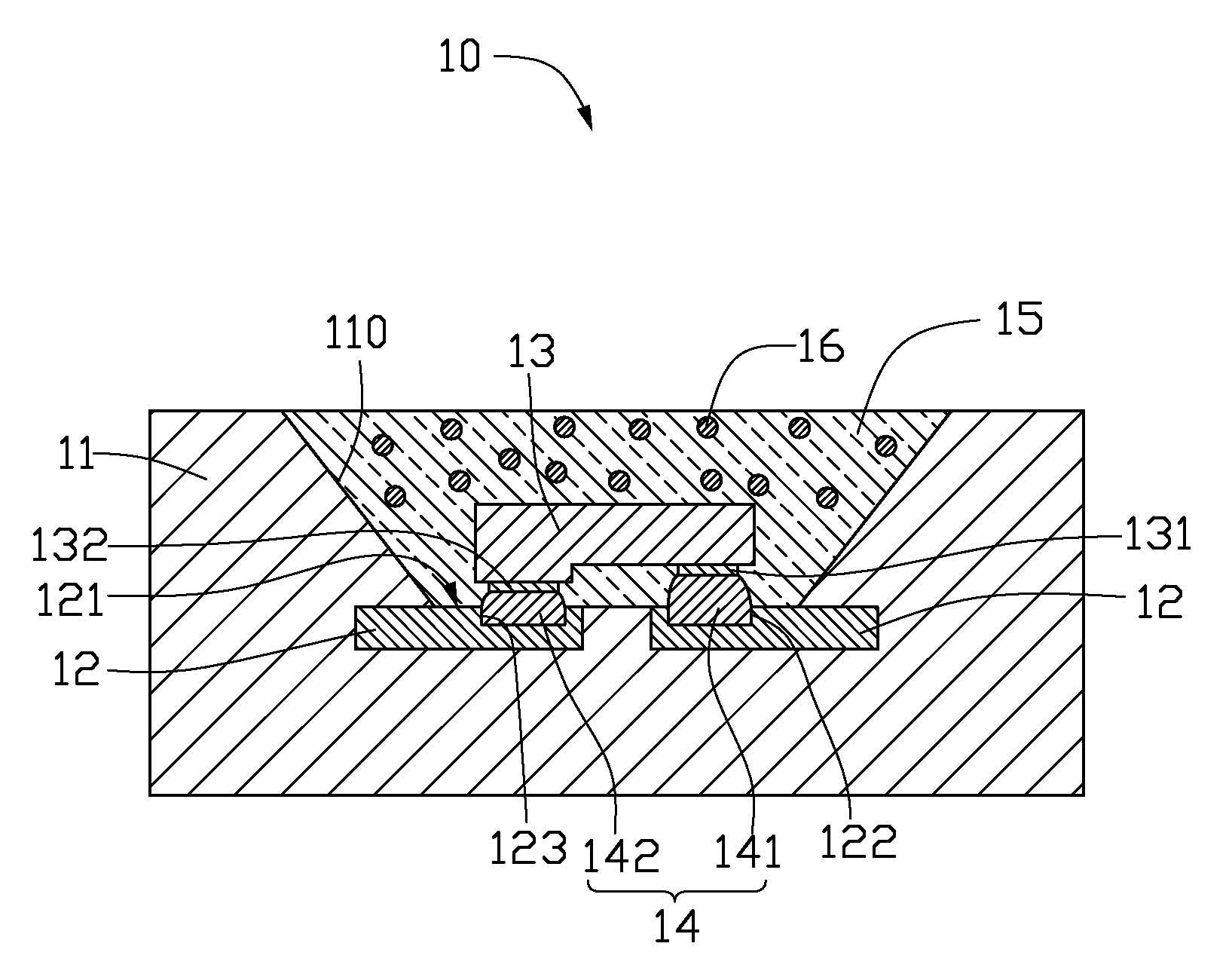
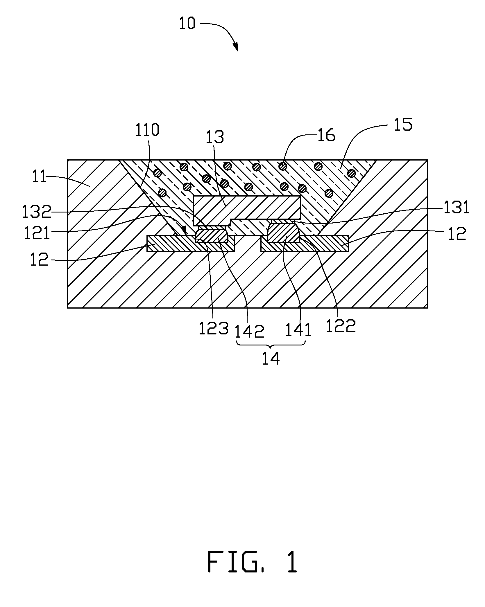
[0014]Referring to FIG. 1, a first embodiment of a flip-chip light emitting diode (LED) 10 is provided. The flip-chip LED 10 includes a housing 11, a substrate 12, and an LED chip 13, a plurality of conductive bumps 14, and an encapsulant 15.

[0015]The housing 11 has a cavity 110. The material of the housing may be a liquid crystal polymer or plastics.

[0016]The substrate 12 is positioned on a bottom of the cavity 110 for accommodating the LED chip 13. The substrate 12 holds the LED chip 13 and may be electrically connected with a power supply (not shown) to supply electrical power to the LED chip 13. In the illustrated embodiment, the substrate 12 may be a lead frame, which is made of high conductivity metal, such as gold (Au), silver (Ag), copper (Cu), or any other metal. The substrate 12 has an interface surface 121 exposed on the bottom of the cavity 110, and a first recess 122 and a substantially symmetrical juxtaposed second recess 123 defined in the interface surface 121 of the...


PUM


Abstract

A flip-chip light emitting diode includes a substrate, an LED chip and a plurality of conductive bumps. The substrate has at least one recess defined in the surface of the substrate, and at least a part of the conductive bumps is embedded the at least one recess. The LED chip is mounted on a surface of the substrate by a flip-chip mounting process. The conductive bumps are sandwiched between the substrate and the LED chip to bond and electrically connect the LED chip to the substrate.

Description

BACKGROUND[0001]1. Technical Field[0002]The disclosure relates to flip-chip light emitting diodes (LEDs) and fabrication methods thereof, and more particularly, to a flip-chip LED with a stable and secure connection between a chip and a submount, and a method for fabricating the flip-chip LED.[0003]2. Description of Related Art[0004]A flip-chip semiconductor package refers to a package structure using a flip-chip technique to electrically connect an active surface of a chip to a surface of a structure via a plurality of conductive bumps. A plurality of solder balls are implanted on another surface of the substrate and serves as input / output (I / O) connections to allow the chip to be electrically connected to an external device. In the above arrangement, the size of the semiconductor package can be significantly reduced such that the chip may be made dimensionally closer to that of the substrate, and the semiconductor package does not require bonding wires, thereby reducing impedance ...

Claims


Application Information

Patent Timeline
IPC IPC(8): H01L33/00H01L21/768H01L33/44H01L33/62
CPCH01L24/81H01L33/44H01L2924/12041H01L33/62H01L2224/16H01L2924/01013H01L2924/01029H01L2924/01033H01L2924/01049H01L2924/01079H01L2924/01082H01L2924/01005H01L2924/01023H01L2924/01047H01L2924/0105H01L2924/10329H01L24/17H01L2224/73204H01L2224/83192H01L2224/14051H01L2224/16237H01L2224/81191H01L2224/0401H01L2224/06102H01L2924/00H01L2224/1403H01L2224/1703
Inventor CHEN, TUNG-ANHSU, CHIH-PENGCHANG, CHUNG-MINLEE, TSE-AN
Owner ADVANCED OPTOELECTRONICS TECH
Why Eureka
Try Eureka