
Method of producing circuit board by additive method, and circuit board and multilayer circuit board obtained by the method

a technology of additive method and circuit board, which is applied in the direction of inspection/indentification of circuits, conductive pattern formation, and catalyst application resists, etc., can solve the problems of short circuiting and migration between wires, deterioration of mechanical strength of wiring, and circuits more vulnerable to circuit breakage, so as to achieve high-precision preservation of circuit profiles

Inactive Publication Date: 2009-11-05
PANASONIC CORP
View PDF12 Cites 20 Cited by
  • Summary
  • Abstract
  • Description
  • Claims
  • Application Information

AI Technical Summary

Benefits of technology

[0020]An object of an aspect of the present invention is to provide a method of producing a circuit board that allows highly accurate preservation of the circuit profile and gives a circuit having a desired depth in preparation of a fine circuit by additive method.

Problems solved by technology

There are problems, such as short circuiting and migration between wires, frequently found in high-density wiring circuit.
In addition, narrow-width wiring leads to deterioration in mechanical strength of wiring, making the resulting circuits more vulnerable to circuit breakage, for example, by impact.
Further, it is difficult to form a fine circuit, because the size of recesses and projections on a flat surface where the circuit is to be fabricated is increased resulting from an increase in the number of laminated layers.
The metal in the region removed is only wasted by the method.
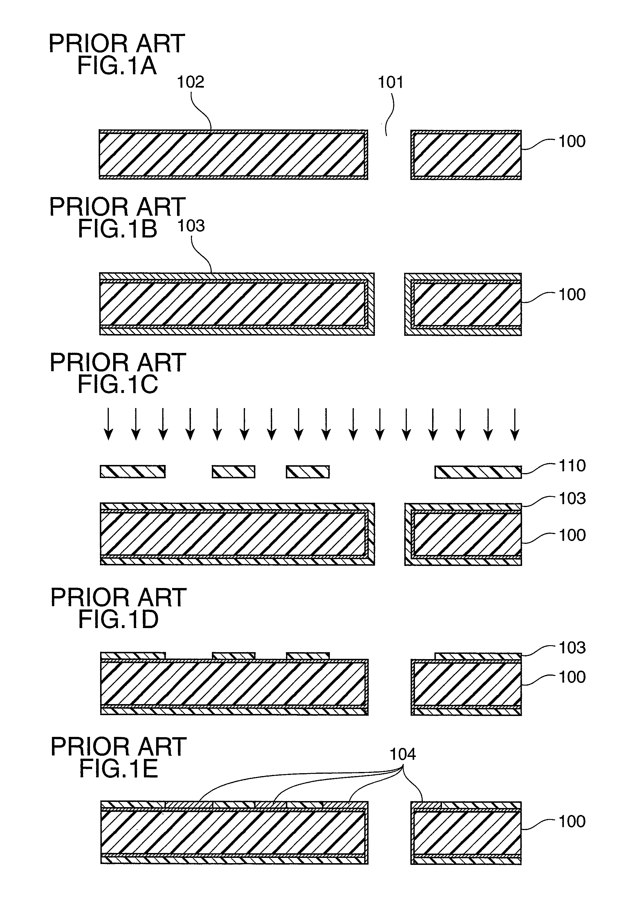
As a result, it caused the following problem.
Such a trouble occurs, because the plating catalyst 102 is deposited on the entire surface of the insulative substrate 100.
Common thermosetting resins are higher in solvent resistance and thus, had a problem that the resins are hardly removed simply with a solvent.
Such a thermosetting resin is often excessively adhesive to the resinous substrate, making it difficult to separate only the protective film reliably without leaving fragments of the protective film on the resinous substrate surface.
In addition, use of a strong solvent or immersion for a prolonged period of time occasionally resulted in fragmentation of the protective film of thermosetting resin and redispersion of the plating catalyst of protective film into the solvent.
For that reason, it was difficult to form a circuit having an accurate pattern by the method disclosed in Patent Document 1.
However, such a method demands preparation of two kinds of photosensitive resin layer different in solvent solubility, development thereof with two kinds of solvents, and solubilization of the second photosensitive resin with an alkaline solution after adsorption of catalyst, and thus, the production process was very complicated.
Preparation of an electrical circuit having narrow line width and line interval by using the circuit-forming method described above also caused the following problem: Specifically, decrease in line width and line interval of the circuit leads to deterioration in wire strength.
The deterioration in wire strength in turn leads to deterioration in reliability of the resulting electronic devices.
Portable information systems are often exposed to impacts, while they are carried.
Exposure to such an impact makes a physical force applied to the LSI mounted, possibly damaging the metal wires constituting the land regions by breakage.
Similarly, the LSIs may also be damaged by separation of the contact points between the LSIs and the substrate.
Decrease in line width and line interval of the electrical circuit leads to increase in frequency of circuit damage.
However, such a method prohibits increase in circuit density.
The thickness of the metal wires in the circuit obtained by the subtractive method depends on the thickness of the copper foil used, and thus, it is also not possible to reinforce the metal wires by thickening the film.
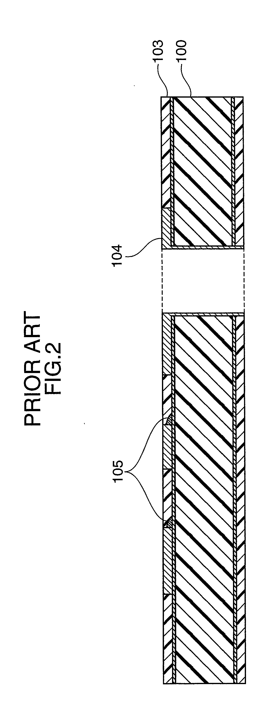
The resin smear 305 remaining on the bottom of IVH 304 may possibly cause conductivity troubles.

Method used


Image

  • Method of producing circuit board by additive method, and circuit board and multilayer circuit board obtained by the method
  • Method of producing circuit board by additive method, and circuit board and multilayer circuit board obtained by the method
  • Method of producing circuit board by additive method, and circuit board and multilayer circuit board obtained by the method

Examples


first embodiment (

Method of Producing a Circuit Board by Using Swellable Resin Film)

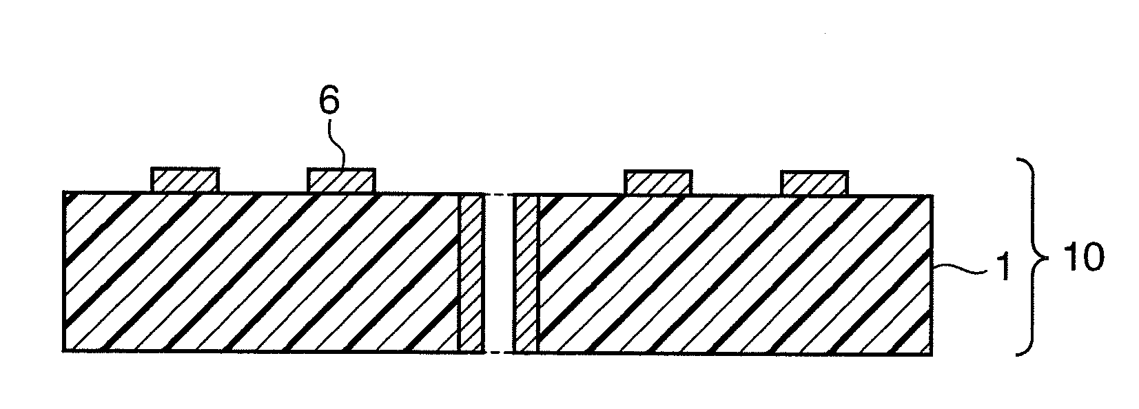
[0050]The method of producing a circuit board in the present embodiment will be described with reference to diagrams. FIGS. 5A to 5E are schematic cross-sectional views explaining the steps in the method of producing a circuit board in the first embodiment. In FIGS. 5A to 5E, 1 represents an insulative substrate; 2 represents a swellable resin film; 3 represents a circuit groove; 4 represents a through-hole penetrating through part of the circuit groove 3; 5 represents a plating catalyst; and 6 represents an electrolessly plated film.

[0051]In the production method of the present embodiment, as shown in FIG. 5A, a swellable resin film 2 is first formed on the surface of an insulative substrate 1. The swellable resin film means a resin film easily separated from the substrate surface by swelling with a particular liquid.

[0052]Various organic substrates used in production of circuit boards can be used as the insulative s...

example 1

[0090]A styrene-butadiene copolymer (SBR) film of 2 μm in thickness was formed on the surface of an epoxy resin substrate having a thickness of 100 μm (R1766, manufactured by Panasonic Electric Works Co., Ltd.). The film was formed by coating a styrene-butadiene copolymer (SBR) suspension in methylethylketone (MEK) (manufactured by Zeon Corporation, acid equivalents: 600, particle diameter: 200 nm, solid matter: 15%) on the main face of the epoxy resin substrate and drying the resulting coating film at 80° C. for 30 minutes.

[0091]Grooves having an almost rectangular cross section having a width of 20 μm and a depth of 30 μm and a particular pattern were formed on the epoxy resin substrate carrying the formed film by laser processing. MODEL 5330 manufactured by ESI equipped with a UV-YAG laser was used in the laser processing.

[0092]The laser-processed epoxy resin substrate was then immersed in a cleaner conditioner (surfactant solution of pH<1, C / N3320, manufactured by Rohm and Haas ...

second embodiment (

Method of Forming a Partial Reinforcing Structure in Fine Wiring)

[0100]It is possible to form a partial reinforcing structure for partial reinforcement of the circuit as will be described below by applying the method of producing a circuit board described in the first embodiment.

[0101]The method of producing a circuit board in the present embodiment will be described specifically with reference to drawings. Items common to those in the description of the first embodiment are described only briefly for prevention of duplication.

[0102]FIGS. 7A to 7E are schematic cross-sectional views respectively explaining the steps in the method of producing a circuit board in the second embodiment.

[0103]In the production method of the present embodiment, first as shown in FIG. 7A, a resin film 12 is formed on the surface of an insulative substrate 1.

[0104]Various organic substrates similar to those described in the first embodiment may be used as the insulative substrate 1. The resin film 12 is fo...


PUM

PropertyMeasurementUnit
Fractionaaaaaaaaaa
Fractionaaaaaaaaaa
Thicknessaaaaaaaaaa

Abstract

An object of an aspect of the present invention is to provide a method of producing a circuit board that allows highly accurate preservation of the circuit profile and gives a circuit having a desired depth in preparation of a fine circuit by additive process.The method of producing a multilayer circuit board in an aspect of the present invention includes a film-forming step of forming a swellable resin film on the surface of an insulative substrate, a circuit groove-forming step of forming circuit grooves having a depth equal to or greater than the thickness of the swellable resin film on the external surface of the swellable resin film, a catalyst-depositing step of depositing a plating catalyst or the precursor thereof on the surface of the circuit grooves and the surface of the swellable resin film, a film-separating step of swelling the swellable resin film with a particular liquid and then separating the swollen resin film from the insulative substrate surface, and a plating processing step of forming an electrolessly plated film only in the region where the plating catalyst or the plating catalyst formed from the plating catalyst precursor remains unseparated after separation of the swellable resin film.

Description

TECHNICAL FIELD[0001]The present invention relates to a method of producing a circuit board by additive method and a circuit board and a multilayer circuit board obtained by the method.BACKGROUND ART[0002]Recently, there is a rapid increase in functionality of electrical apparatuses including portable information systems such as cellphone; computer and its peripheral devices; various home information appliances, and others. Along with the trend, there is also an increasing demand for improvement in density of the circuit on the circuit board used in these electrical apparatuses. For improvement in density of such a circuit, needed is a method of producing circuits having narrower line width and line interval accurately. There are problems, such as short circuiting and migration between wires, frequently found in high-density wiring circuit. In addition, narrow-width wiring leads to deterioration in mechanical strength of wiring, making the resulting circuits more vulnerable to circu...

Claims


Application Information

Patent Timeline
IPC IPC(8): H05K1/02H05K3/00
CPCH05K1/0206Y10T29/49155H05K1/0269H05K1/0284H05K1/11H05K1/162H05K3/0014H05K3/0032H05K3/107H05K3/184H05K3/381H05K3/4069H05K3/4647H05K3/4661H05K2201/09381H05K2201/096H05K2201/09736H05K2201/2072H05K2203/0108H05K2203/0565H05K2203/161H01L2224/48091H01L2224/48227H01L2224/49171H01L2924/15173H01L2924/15311H05K1/023Y10T29/4913Y10T29/49156Y10T29/49128Y10T29/49165H01L2924/00014H01L2924/00
Inventor YOSHIOKA, SHINGOFUJIWARA, HIROAKI
Owner PANASONIC CORP
Learn More