
Method of producing circuit board by additive method, and circuit board and multilayer circuit board obtained by the method

Inactive Publication Date: 2009-11-05
PANASONIC CORP
View PDF8 Cites 40 Cited by
  • Summary
  • Abstract
  • Description
  • Claims
  • Application Information

AI Technical Summary

Benefits of technology

[0020]An object of an aspect of the present invention is to provide a method of producing a circuit board that allows highly accurate preservation of the circuit profile and gives a circuit having a desired depth in preparation of a fine circuit by additive method.

Problems solved by technology

There are problems, such as short circuiting and migration between wires, frequently found in high-density wiring circuit.
In addition, narrow-width wiring leads to deterioration in mechanical strength of wiring, making the resulting circuits more vulnerable to circuit breakage, for example, by impact.
The metal in the region removed is only wasted by the method.
As a result, it caused the following problem.
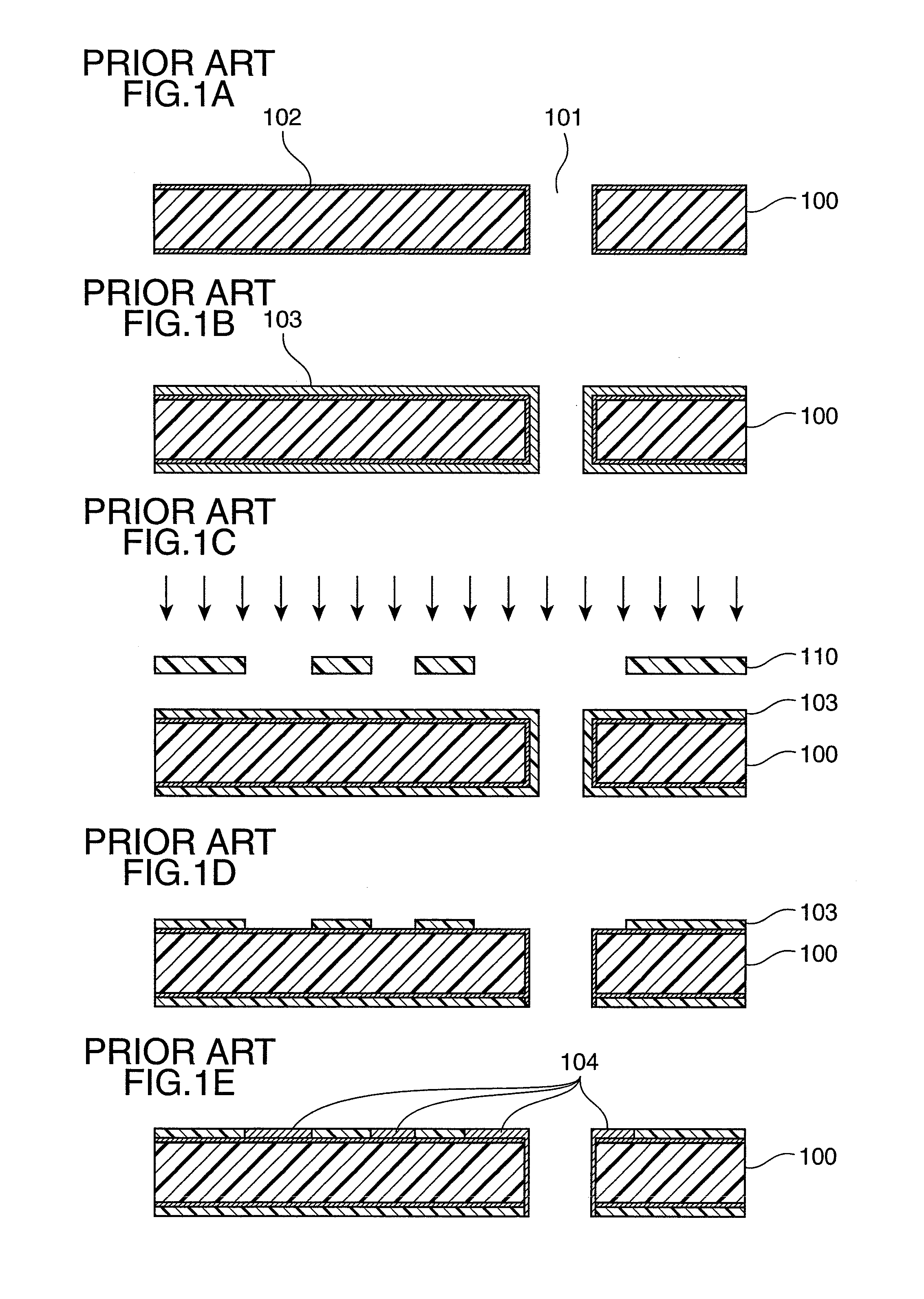
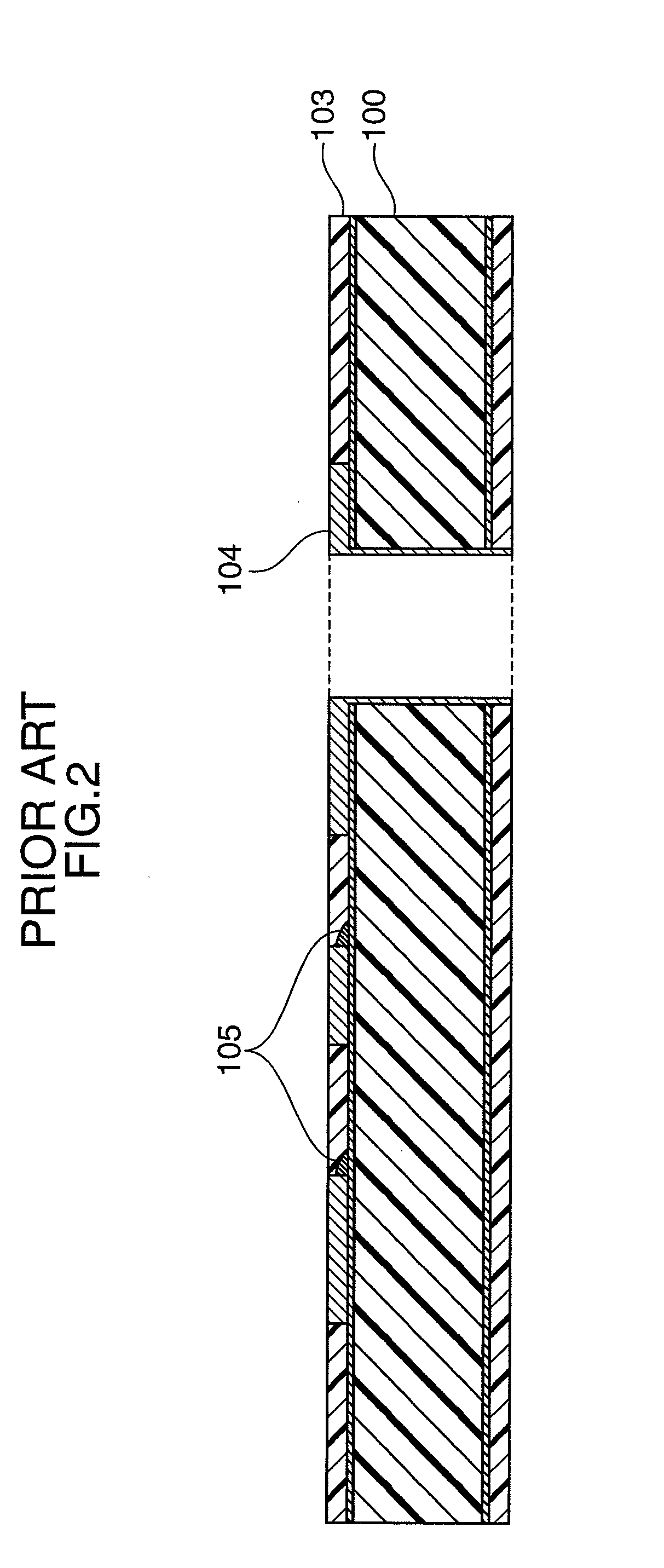
Such a trouble occurs, because the plating catalyst 102 is deposited on the entire surface of the insulative substrate 100.
Common thermosetting resins are higher in solvent resistance and thus, had a problem that the resins are hardly removed simply with a solvent.
Such a thermosetting resin is often excessively adhesive to the resinous substrate, making it difficult to separate only the protective film reliably without leaving fragments of the protective film on the resinous substrate surface.
In addition, use of a strong solvent or immersion for a prolonged period of time occasionally resulted in fragmentation of the protective film of thermosetting resin and redispersion of the plating catalyst of protective film into the solvent.
For that reason, it was difficult to form a circuit having an accurate pattern by the method disclosed in Patent Document 1.
However, such a method demands preparation of two kinds of photosensitive resin layer different in solvent solubility, development thereof with two kinds of solvents, and solubilization of the second photosensitive resin with an alkaline solution after adsorption of catalyst, and thus, the production process was very complicated.
Preparation of an electrical circuit having narrow line width and line interval by using the circuit-forming method described above also caused the following problem: Specifically, decrease in line width and line interval of the circuit leads to deterioration in wire strength.
The deterioration in wire strength in turn leads to deterioration in reliability of the resulting electronic devices.
Portable information systems are often exposed to impacts, while they are carried.
Exposure to such an impact makes a physical force applied to the LSI mounted, possibly damaging the metal wires constituting the land regions by breakage.
Similarly, the LSIs may also be damaged by separation of the contact points between the LSIs and the substrate.
Decrease in line width and line interval of the electrical circuit leads to increase in frequency of circuit damage.
However, such a method prohibits increase in circuit density.
The thickness of the metal wires in the circuit obtained by the subtractive method depends on the thickness of the copper foil used, and thus, it is also not possible to reinforce the metal wires by thickening the film.
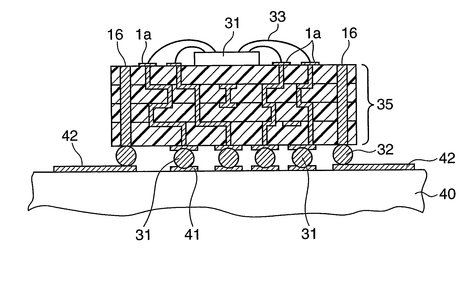
The resin smear 305 remaining on the bottom of IVH 304 may possibly cause conductivity troubles.

Method used


Image

  • Method of producing circuit board by additive method, and circuit board and multilayer circuit board obtained by the method
  • Method of producing circuit board by additive method, and circuit board and multilayer circuit board obtained by the method
  • Method of producing circuit board by additive method, and circuit board and multilayer circuit board obtained by the method

Examples


second embodiment (

METHOD OF FORMING A PARTIAL REINFORCING STRUCTURE IN FINE WIRING)

[0087]It is possible to form a partial reinforcing structure for partial reinforcement of the circuit as will be described below by applying the method of producing a circuit board described in the first embodiment.

[0088]The method of producing a circuit board in the present embodiment will be described specifically with reference to drawings. Items common to those in the description of the first embodiment are described only briefly for prevention of duplication.

[0089]FIGS. 7A to 7E are schematic crosssectional views respectively explaining the steps in the method of producing a circuit board in the second embodiment.

[0090]In the production method of the present embodiment, first as shown in FIG. 7A, a resin film 12 is formed on the surface of an insulative substrate 1.

[0091]Various organic substrates similar to those described in the first embodiment may be used as the insulative substrate 1. The resin film 12 is for...

third embodiment (

METHOD OF PRODUCING A CAPACITOR-CONTAINING CIRCUIT BOARD HAVING A THREE-DIMENSIONAL CAPACITOR STRUCTURE THEREIN)

[0111]As will be described below, it is also possible to form a capacitor-containing circuit board having a three-dimensional capacitor structure therein, by applying the method of producing a circuit board described in the first and second embodiments.

[0112]FIGS. 12A to 12E are schematic views respectively explaining the steps in the method of producing a circuit board having a three-dimensional capacitor structure in the third embodiment.

[0113]In the production method in the present embodiment, as shown in FIG. 12A, a resin film 12 is first formed on the surface of an insulative substrate 1.

[0114]As shown in FIG. 12B, capacitor-forming grooves 80 are then formed on the insulative substrate 1, by laser processing from the outermost surface of the resin film 12. Each capacitor-forming groove 80 has two electrode units 80a and 80b facing each other. The two electrode units ...

fourth embodiment (

PRODUCTION OF MULTILAYER WIRING CIRCUIT)

[0120]The additive method described in FIGS. 3A to FIG. 3E, if it is applied to the build-up method, causes the problems, as will be described below. The steps in the additive method described with reference to FIGS. 3A to 3E, if it is applied to the build-up method, will be described with reference to the schematic crosssectional views of FIGS. 15A to 15E.

[0121]First as shown in FIG. 15A, a metal wiring 301 is formed on the surface of an insulative substrate 300. Then as shown in FIG. 15B, an insulation resin layer 200 is formed on the surface of the insulative substrate 300. As shown in FIG. 15C, a protective film 201 is then coated on the surface of the insulation resin layer 200. As shown in FIG. 15D, circuit grooves 202 and throughhole 203 corresponding to a wiring pattern are formed by laser processing on the insulation resin layer 200 carrying the protective film 201 coated. There is a resin smear 305 remaining then on the bottom of the...


PUM

PropertyMeasurementUnit
Fractionaaaaaaaaaa
Thicknessaaaaaaaaaa
Widthaaaaaaaaaa

Abstract

An object of an aspect of the present invention is to provide a method of producing a circuit board that allows highly accurate preservation of the circuit profile and gives a circuit having a desired depth in preparation of a fine circuit by additive process.The method of producing a multilayer circuit board in an aspect of the present invention includes a film-forming step of forming a swellable resin film on the surface of an insulative substrate, a circuit groove-forming step of forming circuit grooves having a depth equal to or greater than the thickness of the swellable resin film on the external surface of the swellable resin film, a catalyst-depositing step of depositing a plating catalyst or the precursor thereof on the surface of the circuit grooves and the surface of the swellable resin film, a film-separating step of swelling the swellable resin film with a particular liquid and then separating the swollen resin film from the insulative substrate surface, and a plating processing step of forming an electrolessly plated film only in the region where the plating catalyst or the plating catalyst formed from the plating catalyst precursor remains unseparated after separation of the swellable resin film.

Description

TECHNICAL FIELD[0001]The present invention relates to a method of producing a circuit board by additive method and a circuit board and a multilayer circuit board obtained by the method.BACKGROUND ART[0002]Recently, there is a rapid increase in functionality of electrical apparatuses including portable information systems such as cellphone; computer and its peripheral devices; various home information appliances, and others. Along with the trend, there is also an increasing demand for improvement in density of the circuit on the circuit board used in these electrical apparatuses. For improvement in density of such a circuit, needed is a method of producing circuits having narrower line width and line interval accurately. There are problems, such as short circuiting and migration between wires, frequently found in high-density wiring circuit. In addition, narrow-width wiring leads to deterioration in mechanical strength of wiring, making the resulting circuits more vulnerable to circu...

Claims


Application Information

Patent Timeline
IPC IPC(8): H05K1/00H05K3/10
CPCH01L2224/48091Y10T29/4913H01L2924/15173H01L2924/15311H01L2224/48227Y10T29/49155H05K1/0206H05K1/023H05K1/0284H05K1/11H05K1/162H05K3/0014H05K3/0032H05K3/107H05K3/184H05K3/381H05K3/4069H05K3/4647H05K3/4661H05K2201/09381H05K2201/096H05K2201/09736H05K2203/0108H05K2203/0565Y10T29/49128Y10T29/49126Y10T29/49114Y10T29/49165H01L2924/00014
Inventor YOSHIOKA, SHINGOFUJIWARA, HIROAKI
Owner PANASONIC CORP
Learn More