
Semiconductor integrated circuit, semiconductor integrated circuit control device, load distribution method, load distribution program, and electronic device

a technology of semiconductor integrated circuits and control devices, applied in the direction of instruments, sustainable buildings, computation using denominational number representations, etc., can solve the problems of reducing the useful life of the cpu, difficult to smooth the load on the cpus, and shortened use life of the cpu, so as to improve the useful life of the semiconductor integrated circuit, the damage to the semiconductor integrated circuit can be smoothed, and the load distribution is accurate

Inactive Publication Date: 2009-10-29
NEC CORP
View PDF9 Cites 2 Cited by
  • Summary
  • Abstract
  • Description
  • Claims
  • Application Information

AI Technical Summary

Benefits of technology

[0024]According to the present invention, since the execution environment, including the OS, itself can be moved to enable a more accurate load distribution of arithmetic units and the cumulative damages to the arithmetic units can be controlled for each arithmetic unit, the damage to the semiconductor integrated circuit can be more smoothed, so that the useful life of the semiconductor integrated circuit can be prolonged.
[0025]The reason therefor is that the damage control unit that controls the execution environment switching among the plurality of arithmetic units capable of operating by means of a program calculates the conditions of the loads on the arithmetic units and switches the execution environments operating on the arithmetic units based on the result of the calculation.

Problems solved by technology

However, since the increase in the load on the semiconductor integrated circuits, such as the current density or the number of times of switching of the circuit, involved in the performance enhancement imposes an extremely heavy burden on semiconductor devices, the semiconductor devices cannot avoid becoming fatigued, so that the useful lives thereof are shortened.
Firstly, when there is an application or the like fixedly assigned to a CPU for the load distribution at application level, it is difficult to smooth the loads on the CPUs.
Secondly, the load measurement at application level is not directly related to the degree of fatigue (damage ratio) of the CPU.
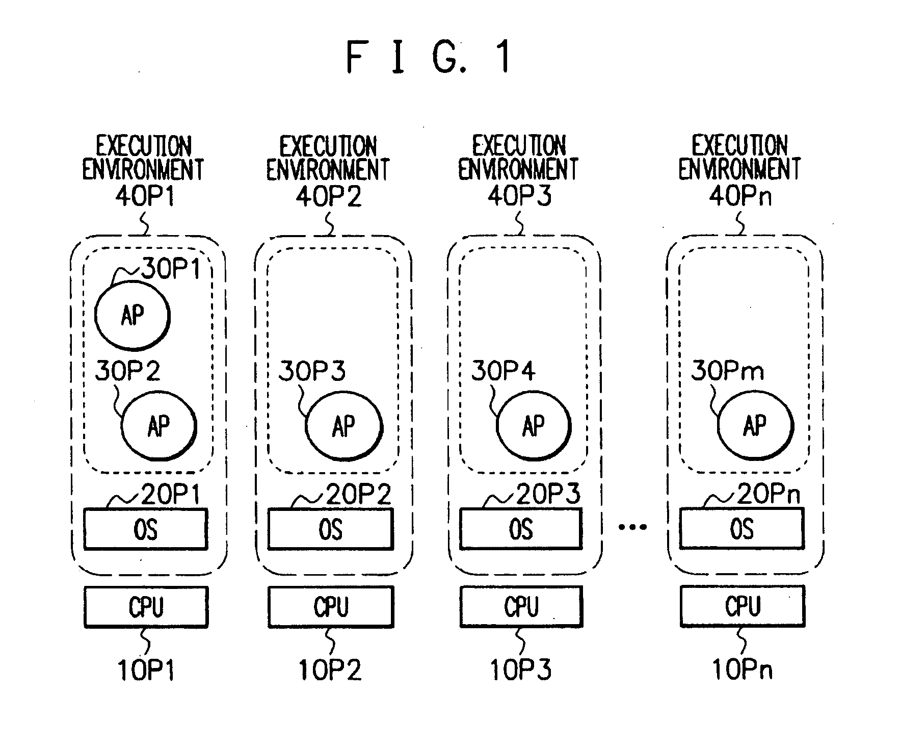
However, the method shown in FIG. 2 has the following problems in addition to the problems shown in FIG. 1.
Firstly, since the CPU that performs power control is fixed, it is difficult to reduce the damage to the CPU.

Method used


Image

  • Semiconductor integrated circuit, semiconductor integrated circuit control device, load distribution method, load distribution program, and electronic device
  • Semiconductor integrated circuit, semiconductor integrated circuit control device, load distribution method, load distribution program, and electronic device
  • Semiconductor integrated circuit, semiconductor integrated circuit control device, load distribution method, load distribution program, and electronic device

Examples


first exemplary embodiment

[0032]A first exemplary embodiment of the present invention will be described in detail with reference to the drawings. In the present embodiment, the execution environment is switched so that the damage is equalized among the CPUs.

[0033](Structure of the First Exemplary Embodiment)

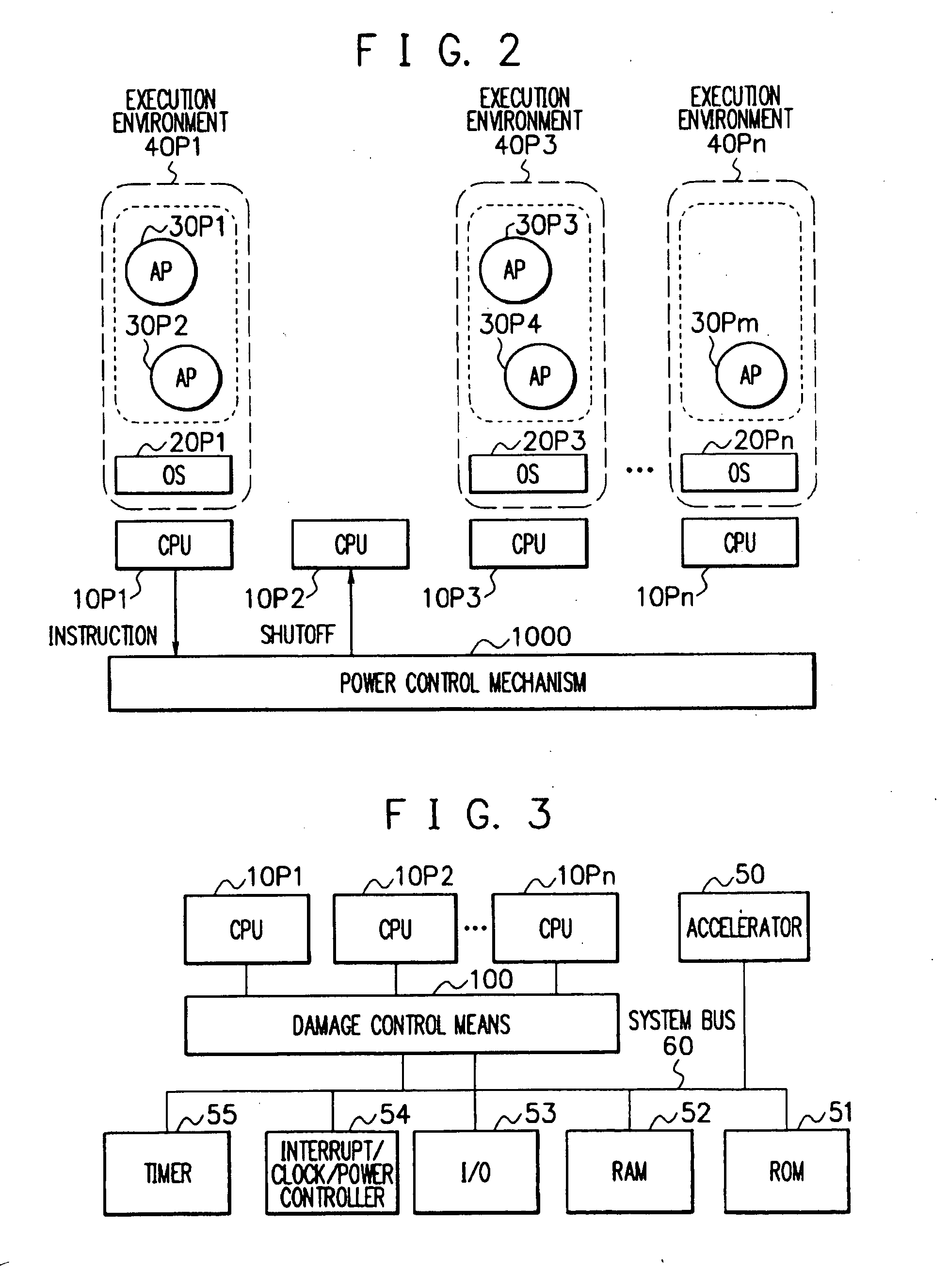
[0034]FIG. 3 is a block diagram showing the structure of a damage control device of a semiconductor integrated circuit according to the first exemplary embodiment of the present invention.

[0035]Referring to FIG. 3, the damage control device of the semiconductor integrated circuit of the present embodiment is provided with the damage control means 100 for performing damage control of a plurality of CPUs in addition to the semiconductor integrated circuit including the CPUs 10P1 to 10Pn, the accelerator 50, the ROM 51, the RAM 52, the input / output (I / O) 53, the interrupt / clock / power controller 54 and the timer 55, connected through the system bus 60.

[0036]The CPUs 10P1 to 10Pn, the accelerator 50, the ROM 5...

second exemplary embodiment

[0097]Next, a damage control device of a semiconductor integrated circuit according to a second exemplary embodiment of the present invention will be described with reference to the drawings. Since the present embodiment is different from the first exemplary embodiment in the damage control means 120, the difference will be mainly described in the following:

[0098](Structure of the Second Exemplary Embodiment)

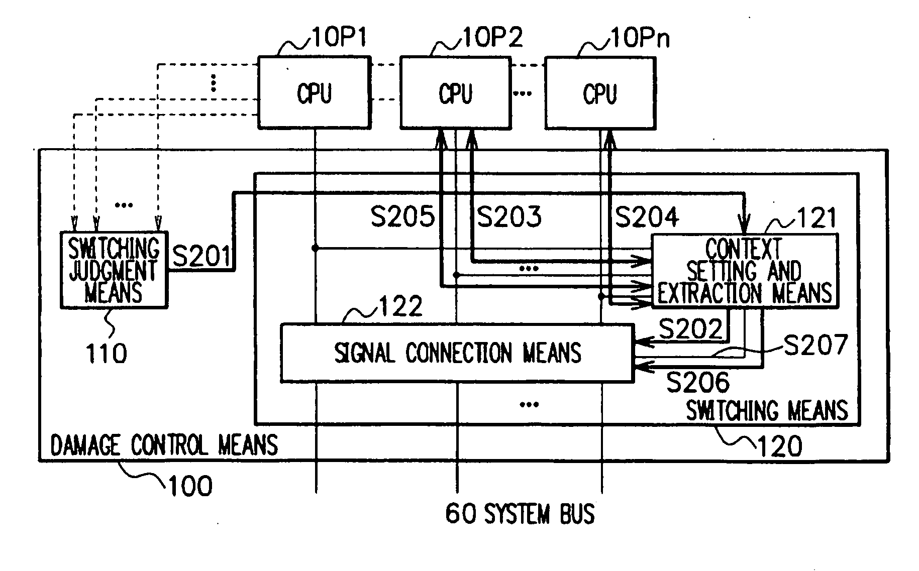
[0099]FIG. 12 is a view showing a structure example of the damage control means of the semiconductor integrated circuit according to the present embodiment.

[0100]Like the damage control means 100 according to the first exemplary embodiment, the damage control means 100 according to the present embodiment is provided with: the switching judgment means 110 including a function to consider the CPU configuration which performs smoothing of the damage ratio, according to the damage ratios of all or some of the CPUs; and the switching means 120 including a function to switch the input...

third exemplary embodiment

[0106]Next, a damage control device of a semiconductor integrated circuit according to a third exemplary embodiment of the present invention will be described with reference to the drawings. Since the present embodiment is different from the first exemplary embodiment in the switching means 120, the difference will be mainly described in the following:

[0107](Structure of the Third Exemplary Embodiment)

[0108]FIG. 13 is a view showing a structure example of the damage control means of the semiconductor integrated circuit according to the present embodiment.

[0109]Like the damage control means 100 according to the first and second exemplary embodiments, the damage control means 100 according to the present embodiment is provided with: the switching judgment means 110 including the function to consider the CPU configuration which performs smoothing of the damage ratio, according to the damage ratios of all or some of the CPUs; and the switching means 120 including the function to switch ...


PUM


Abstract

A damage control unit includes: a switching judgment unit to judge the CPU configuration which performs smoothing of the damage ratio, according to the damage ratio of the CPUs; and a switching unit to perform switching of I / O signals of all the CPUs. The switching judgment unit observes the damage ratio calculated from values such as the temperature, voltage, current consumption amount, operation ratio, the number of accesses to the resources in the CPU, at all times or at some extent of time intervals and notifies the switching unit of the CPU configuration to be changed by using the calculation method for smoothing the damage ratio of each CPU. The switching unit makes a connection to the I / O signals of all the CPUs and a system bus and switches the I / O signal of the CPU to be switched according to the notification from the switching judgment unit.

Description

TECHNICAL FIELD[0001]The present invention relates to a semiconductor integrated circuit including a plurality of CPUs, and more particularly, to a semiconductor integrated circuit, a semiconductor integrated circuit control device, a load distribution method, a load distribution program, and an electronic device capable of improving the reliability of the semiconductor integrated circuit by damage control at the time of a wear-out failure.BACKGROUND ART[0002]Thanks to the development of miniaturization of semiconductors, semiconductor integrated circuits have been enjoying a benefit of performance enhancement. However, since the increase in the load on the semiconductor integrated circuits, such as the current density or the number of times of switching of the circuit, involved in the performance enhancement imposes an extremely heavy burden on semiconductor devices, the semiconductor devices cannot avoid becoming fatigued, so that the useful lives thereof are shortened.[0003]FIG. ...

Claims


Application Information

Patent Timeline
Patent Type & Authority Applications(United States)
IPC IPC(8): G06F9/302G06F9/30
CPCG06F9/5088Y02B60/142G06F2209/5022G06F9/5094Y02D10/00
Inventor INOUE, HIROAKOTAKAGI, MASAMICHIMIZUNO, MASAYUKI
Owner NEC CORP
Learn More