Stacked scr with high holding voltage

Active Publication Date: 2009-09-24
SEMICON COMPONENTS IND LLC
View PDF6 Cites 15 Cited by
  • Summary
  • Abstract
  • Description
  • Claims
  • Application Information

AI Technical Summary

Benefits of technology

[0011]The present invention provides a protective circuit for protecting a target circuit against an ESD event. The protective circuit has an anode connected to a contact on the target circuit and a cathode to be connected to a reference contact on the target circuit. Usually, as mentioned above, the contact on the target circuit is a Vdd or an input / output contact, and the reference contact is usually ground. When and ESD event triggers the protective circuit, the voltage across the contact on the target circuit to the reference contact on the target circuit is limited, thereby protecting the target circuit.

Problems solved by technology

For example, noise generated by the integrated circuits may inadvertently trigger a protection device, e.g. an SCR, and possibly damage the device.
If the protective device is damaged, it may not protect the circuitry intended, and, if inadvertently triggered, it may render the circuitry inoperative.
In this case, the SCRs will hold down the power supply line making the target circuit inoperative.
Here the still on SCR's will compete with the power supply possibly damaging one or the other.
But, in such cases, the triggering voltage also doubles and may be too high.
This dilemma has plagued the SCR circuitry for many years.
This may raise the holding voltage to a suitable level, but the triggering level may become too high requiring other techniques to lower to a useful level.

Method used


Image

  • Stacked scr with high holding voltage
  • Stacked scr with high holding voltage
  • Stacked scr with high holding voltage

Examples


Embodiment Construction

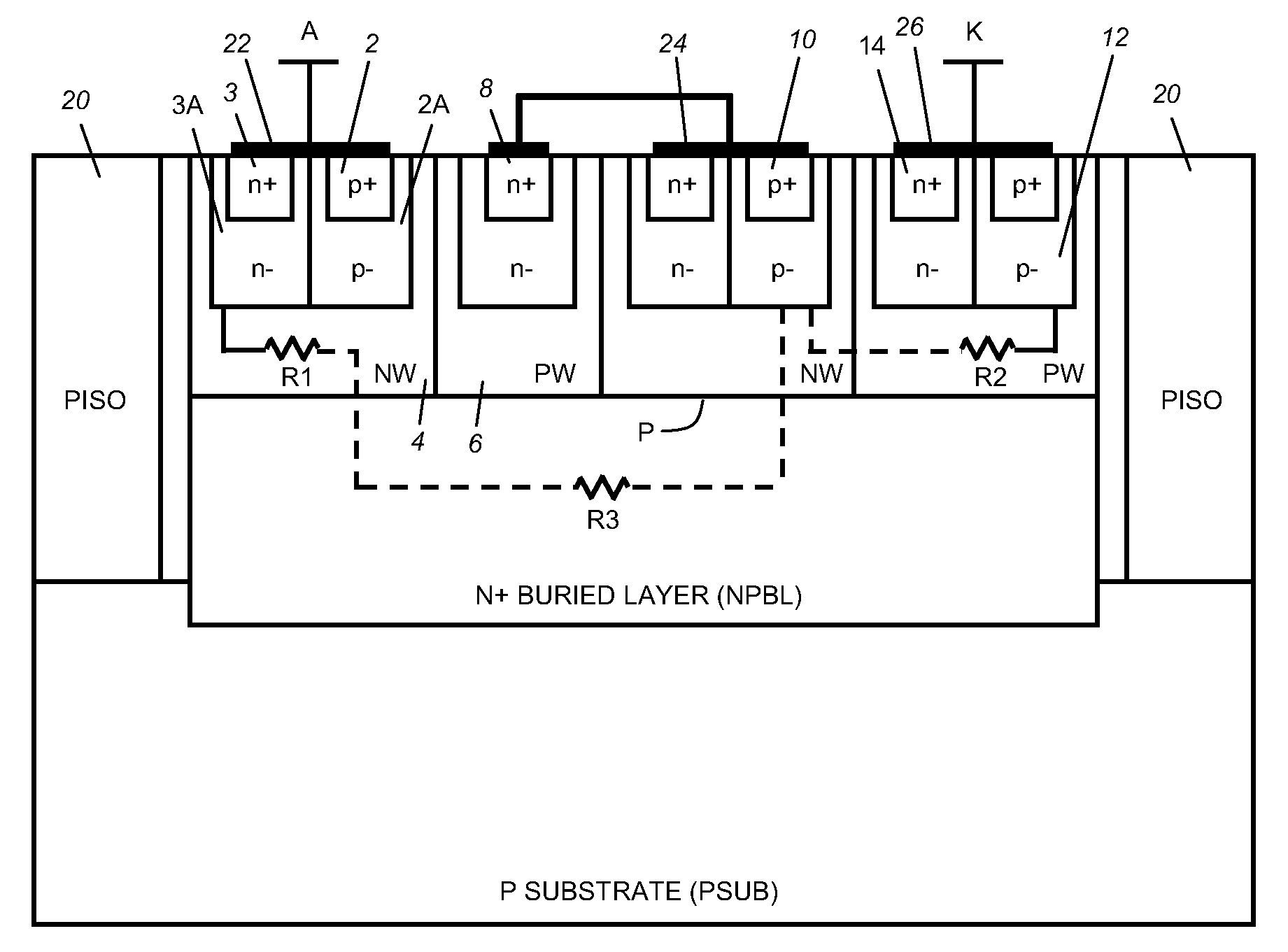
[0022]FIG. 3 is a cross section view of an integrated circuit structure illustrating the present invention, and FIG. 4 illustrates a circuit illustration for the integrated circuit structure of FIG. 3. The circuit components of FIG. 4 are illustrated on FIG. 3, but, as known to those skilled in the art, the cross section integrated circuit to circuit diagram is inexact since points in the circuit diagram are areas in the cross section drawing. However, those skilled in the art will understand the relationship.

[0023]Of note, R3 connects the NW 4 (n-well) to the NW P (p-well) and to points 8 and 10 via metallization. This connection joins an internal point of the top SCR1 and an internal point of the bottom SCR2, and allows the circuit characteristics discussed below.

[0024]Location A is connected to a node in a circuit (not shown) that is to be protected from ESD. Note that when the structure of FIGS. 3 and 4 is off (not triggered) the bipolar transistors shown are all non-conducting ...


PUM


Abstract

Stacked SCR's are disclosed with a resistor connecting an internal portion of the upper SCR to an internal portion of the lower SCR. The anode of the protective circuit is connected to a contact on a target circuit to be protected and the cathode of the protective circuit is connected to ground or a reference voltage on the target circuit. The anode voltage is directed to the lower SCR via the resistor such that when the voltage on the anode reaches the triggering voltage of the lower SCR, that SCR triggers and that triggering triggers the upper SCR, such that the stacked SCR's both trigger and thereby limit the voltage between the anode and the cathode and thereby protecting the target circuit.

Description

BACKGROUND OF THE INVENTION[0001]1. Field of the Invention[0002]The present invention relates to ESD (electrostatic discharge) protection devices, and more particularly to SCR type components that protect a signal line of a target circuit by shunting that line to ground or to a reference point or voltage; and even more particularly to stacking SCRs to protect a target circuit.[0003]2. Background Information[0004]Modern electronic circuitry is smaller, denser and more susceptible to electrostatic discharge events than circuitry of years past. For example, noise generated by the integrated circuits may inadvertently trigger a protection device, e.g. an SCR, and possibly damage the device. If the protective device is damaged, it may not protect the circuitry intended, and, if inadvertently triggered, it may render the circuitry inoperative. Typically when a SCR is triggered, power must be completely removed from the device to reset it back to an off state.[0005]In prior art high voltag...

Claims


Application Information

Patent Timeline
IPC IPC(8): H02H9/00
CPCH01L27/0262
Inventor RYU, JUNHYEONGKANG, TAEGHYUNKIM, MOONHO
Owner SEMICON COMPONENTS IND LLC
Why Eureka
Try Eureka