
Process Control Using Process Data and Yield Data

a technology of process data and yield data, applied in the field of manufacturing process monitoring methods, can solve the problems of inability to maintain viable yields at 65 and 45 nm, inability to use process tools alone to meet all the control needs of advanced device fabrication, and the complexity of manufacturing processes has changed the landscap

Active Publication Date: 2009-09-10
SARTORIUS STEDIM DATA ANALYTICS AB
View PDF6 Cites 11 Cited by
  • Summary
  • Abstract
  • Description
  • Claims
  • Application Information

AI Technical Summary

Benefits of technology

[0006]In one aspect, the invention features a method for monitoring a manufacturing process. The method involves acquiring metrology data for semiconductor wafers at the conclusion of a final process step for the manufacturing process (“Step a”). The method also involves acquiring data for a plurality of process variables for a first process step for manufacturing semiconductor wafers (“Step b”). The method also involves creating a first mathematical model of the first process step based on the metrology data and the acquired data for the plurality of process variables for the first process step (“Step c”). The method also involves repeating steps b and step c for at least a second process step for manufacturing the semiconductor wafers (“Step d”). The method also involves creating an nth mathematical model based on the metrology data and the data for the plurality of process variables for each of the n process steps (“Step e”). The method also involves creating a top level mathematical model based on the metrology data and the models created by steps c, d and e (“Step f”). The top level mathematical model is based on those process variables that have a substantial effect on the metrology data.

Problems solved by technology

As device geometries shrink to the nanometer scale, however, the increasing complexity of manufacturing processes has changed the landscape that must be negotiated to meet and maintain process / materials specifications.
Stand-alone control of process tools (based on equipment state data) will not maintain viable yields at 65 and 45 nm.
Furthermore, tool level control alone cannot meet all of the control needs of advanced device fabrication.
The cost of purchasing (and developing) stand-alone process tools to meet advanced production specifications is expected to be staggering.

Method used


Image

  • Process Control Using Process Data and Yield Data
  • Process Control Using Process Data and Yield Data
  • Process Control Using Process Data and Yield Data

Examples


Embodiment Construction

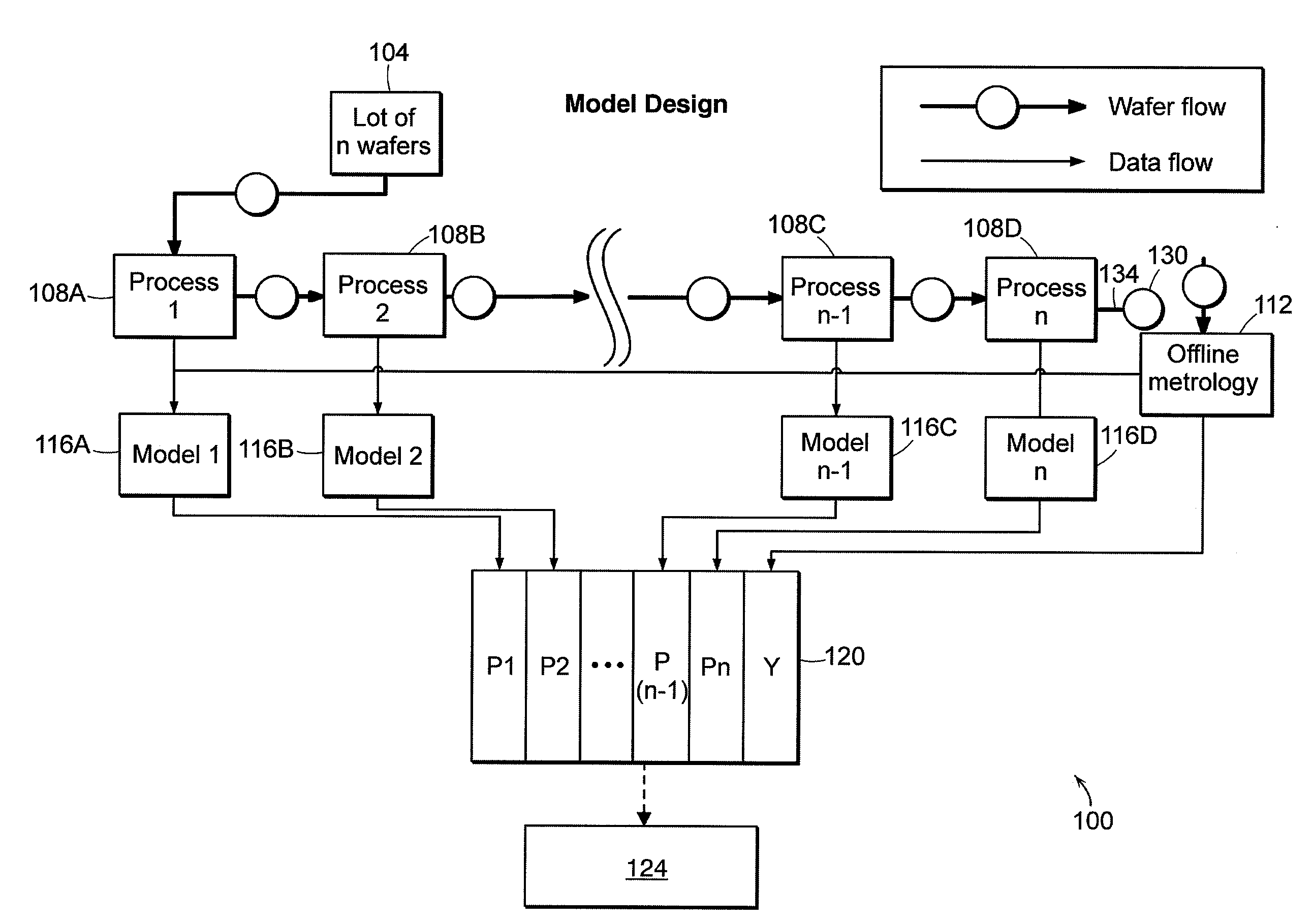
[0021]FIG. 1 is a schematic drawing depicting a method 100 for creating a model for monitoring a manufacturing process for manufacturing a lot of semiconductor wafers 104, according to an illustrative embodiment of the invention. The method 100 involves combining process data and yield data (e.g., metrology data) to create a model for process control of a manufacturing process and yield prediction for a manufacturing process. The manufacturing process includes a plurality of process steps 108A, 108B, 108C or 108D for processing the lot of semiconductor wafers 104. In this embodiment, the manufacturing process includes “n” number of process steps 108A, 108B, 108C or 108D. The method 100 involves acquiring metrology data 112 taken from the final output 134 of the plurality of process steps 108A, 108B, 108C or 108D. In some embodiments, the step 112 involves acquiring data for a plurality of process variables for the output 134. The data acquired for each of the process steps 108A, 108...


PUM


Abstract

A method for monitoring a manufacturing process features acquiring metrology data for semiconductor wafers at the conclusion of a final process step for the manufacturing process (“Step a”). Data is acquired for a plurality of process variables for a first process step for manufacturing semiconductor wafers (“Step b”). A first mathematical model of the first process step is created based on the metrology data and the acquired data for the plurality of process variables for the first process step (“Step c”). Steps b and c are repeated for at least a second process step for manufacturing the semiconductor wafers (“Step d”). An nth mathematical model is created based on the metrology data and the data for the plurality of process variables for each of the n process steps (“Step e”). A top level mathematical model is created based on the metrology data and the models created by steps c, d and e (“Step f”). The top level mathematical model of Step f is based on those process variables that have a substantial effect on the metrology data.

Description

FIELD OF THE INVENTION[0001]The invention generally relates to methods for monitoring a manufacturing process. More particularly, the invention relates to using metrology data and process data to monitor a manufacturing process.BACKGROUND OF THE INVENTION[0002]Historically, semiconductor device manufacturers have managed the transition to tighter process / materials specifications by depending on process tool manufacturers to design better and faster process / hardware configurations. As device geometries shrink to the nanometer scale, however, the increasing complexity of manufacturing processes has changed the landscape that must be negotiated to meet and maintain process / materials specifications.[0003]Stand-alone control of process tools (based on equipment state data) will not maintain viable yields at 65 and 45 nm. Advanced device processing requires tool-level control based on the combination of advanced equipment control (AEC) and sensor based process control. Furthermore, tool l...

Claims


Application Information

Patent Timeline
Patent Type & Authority Applications(United States)
IPC IPC(8): G06F17/18G06F17/10
CPCG05B17/02G05B23/0254G05B2219/11G05B2219/45031G05B2219/32187G05B2219/32201G05B2219/1112G05B2223/02Y02P90/02Y02P90/80
Inventor HENDLER, LAWRENCELIN, KUO-CHINWOLD, SVANTE BJARNE
Owner SARTORIUS STEDIM DATA ANALYTICS AB
Learn More