
Method of cleaning and process for producing semiconductor device

a technology for cleaning and semiconductor devices, applied in semiconductor devices, chemistry apparatuses and processes, detergent compositions, etc., can solve the problems of increasing electricity consumption, reducing the operating speed of semiconductor devices, and unable to remove polishing residues containing cu compounds such as cuo and cuoh

Active Publication Date: 2009-09-03
SONY CORP +1
View PDF7 Cites 1 Cited by
  • Summary
  • Abstract
  • Description
  • Claims
  • Application Information

AI Technical Summary

Benefits of technology

[0022]Under the above circumstances, the present invention has an object of providing a method of cleaning and a process for producing a semiconductor device, in which etching residues and polishing residues comprising metal compounds, in particular, copper compounds, can be selectively removed from the wiring material in the method of cleaning using the supercritical fluid of carbon dioxide.

Problems solved by technology

The increase in the resistance and the capacity of the wiring due to the increasing fineness of the wiring and the decrease in the pitch of the wiring cause a decrease in the operating speed of semiconductor devices and an increase in the consumption of electricity.
However, the polishing residues comprising Cu compounds such as cupper oxide (CuO) and copper hydroxide (CuOH) cannot be removed easily.
When the porous low permittivity insulating film is treated with the aqueous solution-based cleaning agent, problems arise in that water in the aqueous solution-based cleaning agent is absorbed with the film and the permittivity of the film is increased, and that the aqueous solution-based cleaning agent does not penetrate into fine pores due to the surface tension, and contaminating substances in the fine pores cannot be removed.
However, this method of cleaning has drawbacks in that conventional acids, bases and chelating agents which are used in aqueous solutions are not easily dissolved into the supercritical fluid of carbon dioxide since the supercritical fluid of carbon dioxide is apolar (hydrophobic), and that many conventional acids, bases and chelating agents exhibit the function in aqueous solutions but not in the supercritical fluid of carbon dioxide.
In particular, when this method of cleaning is applied to the cleaning of a wiring structure having Cu wiring and the low permittivity insulating film, a problem arises in that additives such as acids, bases and chelating agents and the supercritical fluid of carbon dioxide are separated from each other to cause precipitation of the additives alone on the surface of the Cu wiring and the low permittivity insulating film, and the additives in great concentrations are brought into contact with the Cu wiring and the low permittivity insulating film to cause invasion of the Cu wiring and the low permittivity insulating film.
As another problem, the separated additives are not sufficiently removed (rinsed) from the surface of the Cu wiring and the low permittivity insulating film, and the contamination remains.
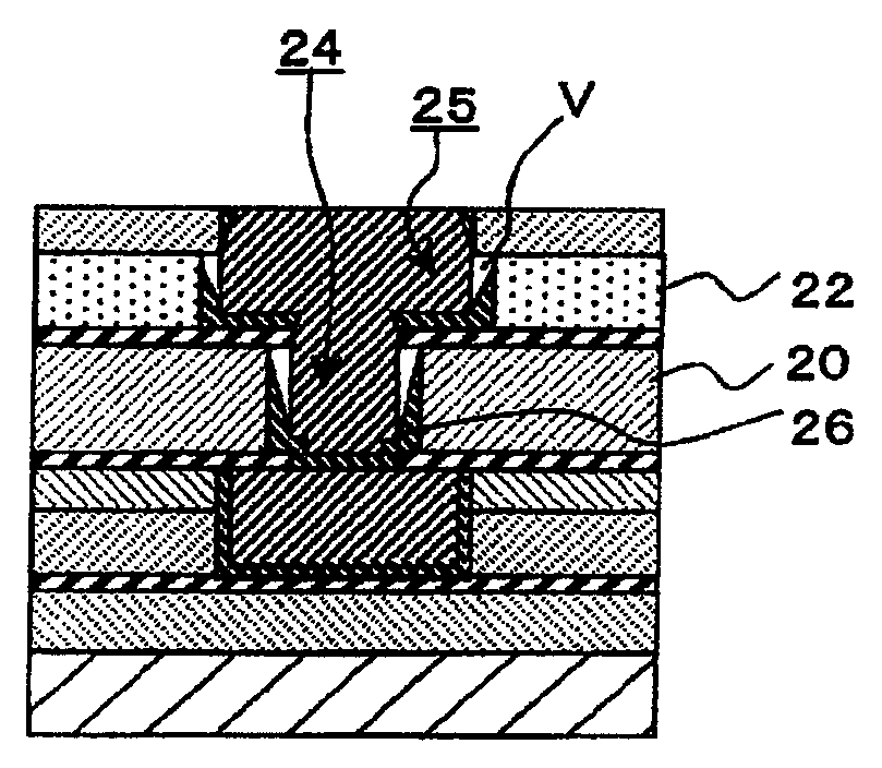
This causes invasion of Cu in the lower wiring during the cleaning, and voids are formed.

Method used


Image

  • Method of cleaning and process for producing semiconductor device
  • Method of cleaning and process for producing semiconductor device
  • Method of cleaning and process for producing semiconductor device

Examples


examples

[0074]The present invention will be described more specifically with reference to examples in the following. However, the present invention is not limited to the examples.

first embodiment

Examples of the First Embodiment

Example 1

[0075]The cleaning treatment was conducted for 10 minutes by supplying a mixture obtained by adding 2% by volume of triallylamine to a supercritical fluid of carbon dioxide at 35° C. under 10 MPa to the surface of board S obtained by removing the etching stopper layer 19 by etching as shown in FIG. 3(h). Then, the rinsing treatment was conducted for 10 minutes by using the supercritical fluid of carbon dioxide alone.

example 2

[0076]The cleaning treatment and the rinsing treatments were conducted in accordance with the same procedures as those conducted in Example 1 except that a mixture obtained by adding 2% by volume of tris(3-aminopropyl)amine to the supercritical fluid of carbon dioxide was supplied.


PUM

PropertyMeasurementUnit
pressureaaaaaaaaaa
temperatureaaaaaaaaaa
electroconductiveaaaaaaaaaa

Abstract

A method of cleaning for removing metal compounds attached to a surface of a substrate, wherein the cleaning is conducted by supplying a supercritical fluid of carbon dioxide comprising at least one of triallylamine and tris(3-aminopropyl)amine to the surface of the substrate and a process for producing a semiconductor device using the method of cleaning are provided. In accordance with the method of cleaning and the method for producing a semiconductor device using the method, etching residues or polishing residues containing metal compounds are efficiently removed selectively from the electroconductive material forming the electroconductive layer. When the electroconductive layer is a wiring, an increase in resistance due to residual metal compounds can be suppressed, and an increase in the leak current due to diffusion of the metal from the metal compounds to the insulating film can be prevented. Therefore, reliability on the wiring is improved, and the yield of the semiconductor device can be increased.

Description

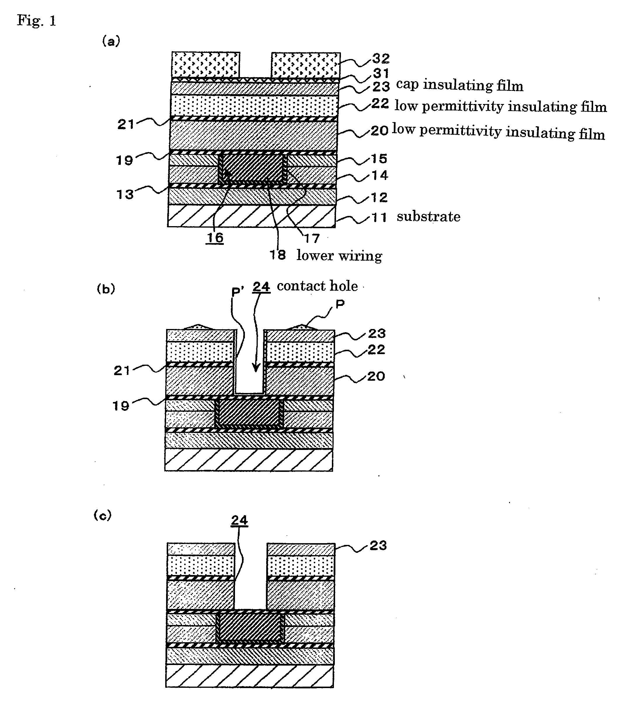
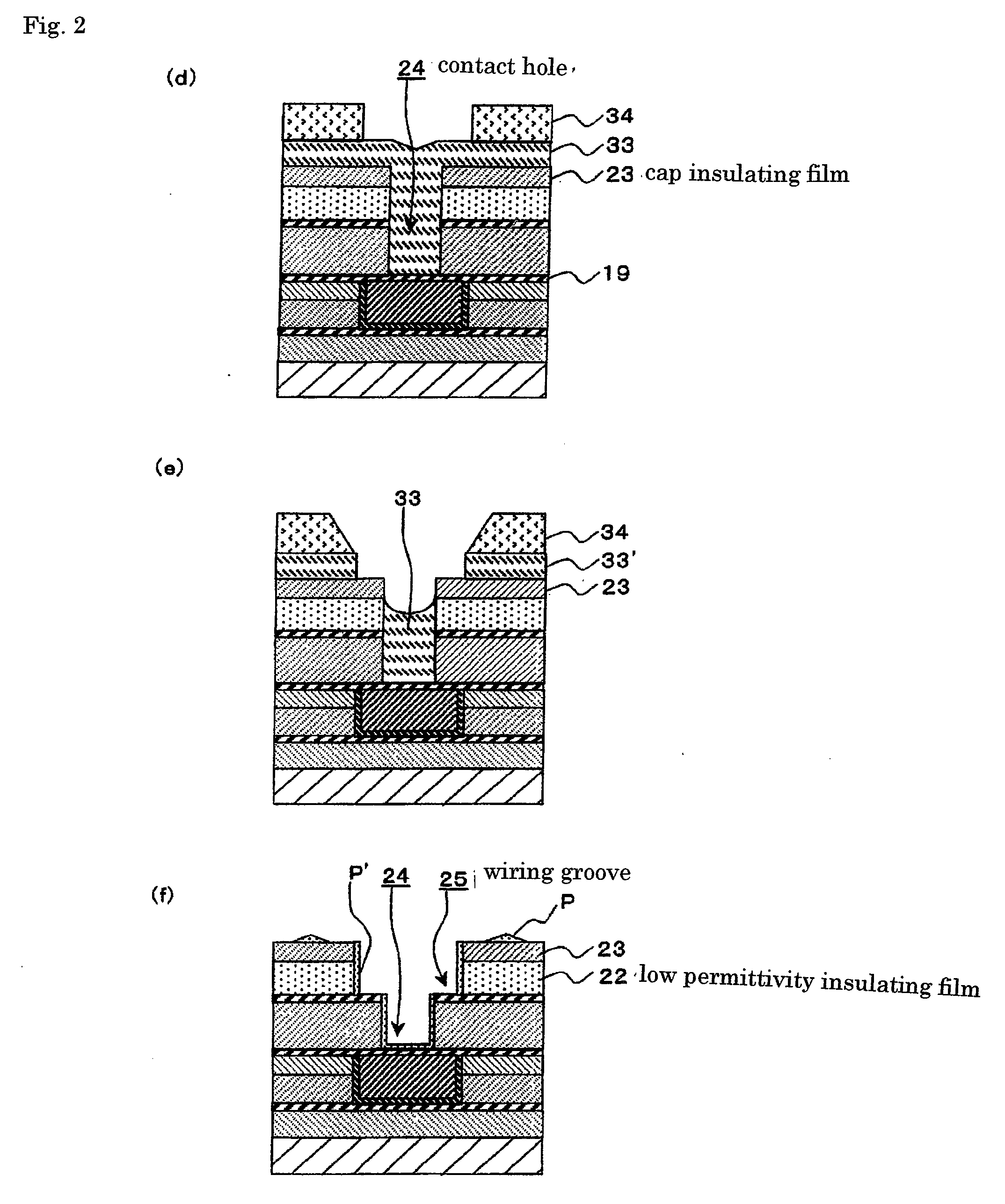
TECHNICAL FIELD[0001]The present invention relates to a method of cleaning and a process for producing a semiconductor device. More particularly, the present invention relates to a method of cleaning in the formation of a wiring structure constituted with a copper wiring and a low permittivity insulating film and a process for producing a semiconductor device using the method of cleaning.BACKGROUND ART[0002]As the semiconductor devices are more highly integrated recently, the processing dimension of a wiring required for forming circuits becomes finer, and a wiring has an increased number of layers. It is also required that consumption of electricity be decreased and the operating speed be increased as the semiconductor devices are more highly integrated. The increase in the resistance and the capacity of the wiring due to the increasing fineness of the wiring and the decrease in the pitch of the wiring cause a decrease in the operating speed of semiconductor devices and an increase...

Claims


Application Information

Patent Timeline
Patent Type & Authority Applications(United States)
IPC IPC(8): H01L21/3205H01L21/306C11D7/32
CPCH01L21/02063H01L21/76808Y10S438/906H01L21/76883H01L21/76814H01L21/304H01L21/768
Inventor SAGA, KOICHIROYAMADA, KENJIAZUMA, TOMOYUKIMURATA, YUJI
Owner SONY CORP
Learn More