Non-volatile memory

a non-volatile memory and memory chip technology, applied in static storage, digital storage, instruments, etc., can solve the problems of data leakage, overly high threshold voltage, and reading/writing errors that tend to occur in subsequent use of non-volatile memory devices, so as to reduce the possibility of data writing/reading errors

Inactive Publication Date: 2009-09-03
MACRONIX INT CO LTD
View PDF5 Cites 2 Cited by
  • Summary
  • Abstract
  • Description
  • Claims
  • Application Information

AI Technical Summary

Benefits of technology

[0011]The memory device also includes a circuit for applying a first voltage to the substrate and a second voltage to both S / D regions of each cell, wherein the difference between the first and second voltages is sufficient to cause band-to-band tunneling hot holes. The circuit further applies a gate voltage to the control gate of each cell and the period of applying the voltages are controlled such that the threshold voltages of all the memory cells converge in a tolerable range through a double-side bias band-to-band tunneling hot-hole (DSB-BTBTHH) effect.
[0015]Unlike the conventional memory device in which the threshold voltages of all cells are reset around the predetermined threshold voltage of the high-Vt state or the low-Vt state, the threshold voltages of all cells of the memory device of this invention are able to converge in a certain range between the predetermined threshold voltages of the high-Vt state and the low-Vt state. By adjusting the duration of the voltages being applied by the circuit to the memory cells, the Vt-distribution obtained with this invention can be narrower than that obtained with the conventional memory cells. Therefore, the possibility of data writing / reading error is reduced in the subsequent use of the non-volatile memory.

Problems solved by technology

Thus, for a non-volatile memory operated in the first mode, a certain amount of positive charges exists in the charge-storing layers of a part of the cells after a certain number of the programming / erasing cycles, which results in a leakage issue.
On the other hand, for a non-volatile memory operated in the second mode, excess electrons are stored in the charge-storing layers of a part of the cells after a certain number of the programming / erasing cycles, which leads to overly high threshold voltages.
Hence, reading / writing error tends to take place in subsequent use of the non-volatile memory device.
However, with such a reset method, the variation between the threshold voltages of all the cells is not small enough so that the possibility of reading / writing error cannot be effectively reduced.

Method used


Image

  • Non-volatile memory
  • Non-volatile memory
  • Non-volatile memory

Examples


second embodiment

[0025]Furthermore, though the non-volatile memory described in the following embodiments is directed to electrons being removed from the charge-storing layer in an erasing operation, a non-volatile memory apparatus that injects electrons for erasing can also be reset according to the first or this invention.

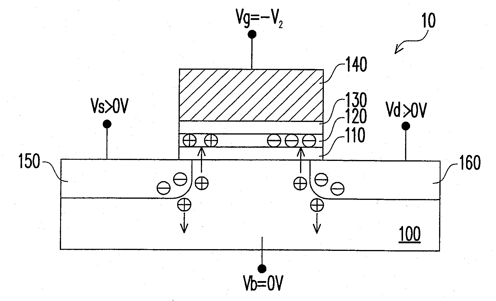
[0026]FIG. 1 shows the voltages applied to different parts of an exemplary memory cell and the resulting effect in the reset method according to the first exemplary embodiment of this invention. The memory cell 10 includes a portion of a P-substrate 100, a bottom oxide layer 110, a nitride layer 120 as a charge-trapping layer, a top oxide layer 130 and a control gate 140 sequentially stacked on the portion of the substrate 100, and an N-type source region 150 and an N-type drain 160 in the substrate 100 beside the control gate 140. The memory cell 10 may have only one data storage region that is the entire region under the control gate 140 or have two data storage regions adjacen...

first embodiment

[0031]Besides, it is understood from the above that in a non-volatile memory having only one data storage region in each memory cell, the cells in the over-erased state, in the high-Vt state(s) and in the normally erased state can also have similar threshold voltages according to this invention.

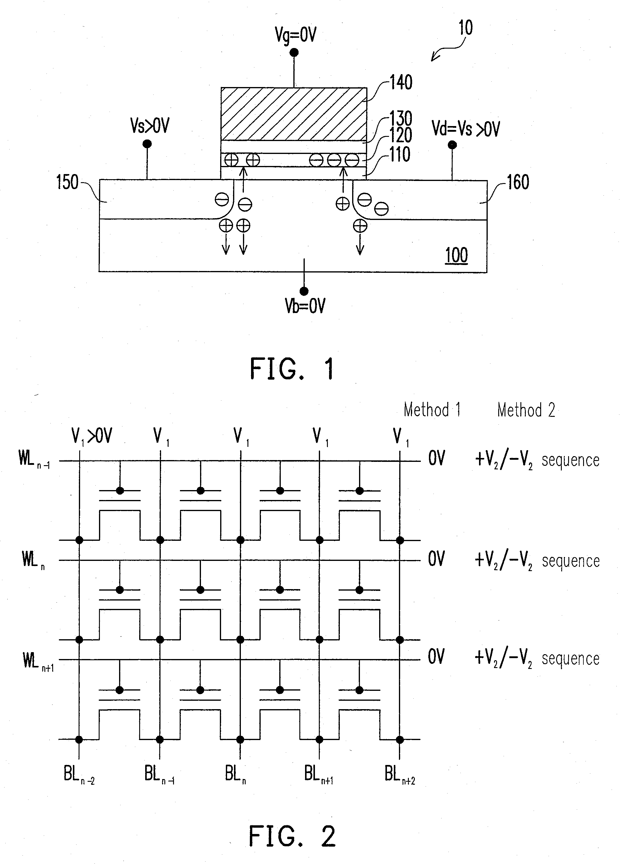
[0032]In FIG. 2, the non-volatile memory is represented by a circuit diagram has a virtual ground array structure. In this example, the substrate and all of the word lines (WL) coupled to the control gates are applied with 0V, and all of the bit lines (BL) coupled to the S / D regions are applied with a voltage V1 that is higher than 0V and is sufficiently high, possibly ranging from 5V to 7V, to cause band-to-band tunneling hot holes. The resulting effect in each memory cell has been described above.

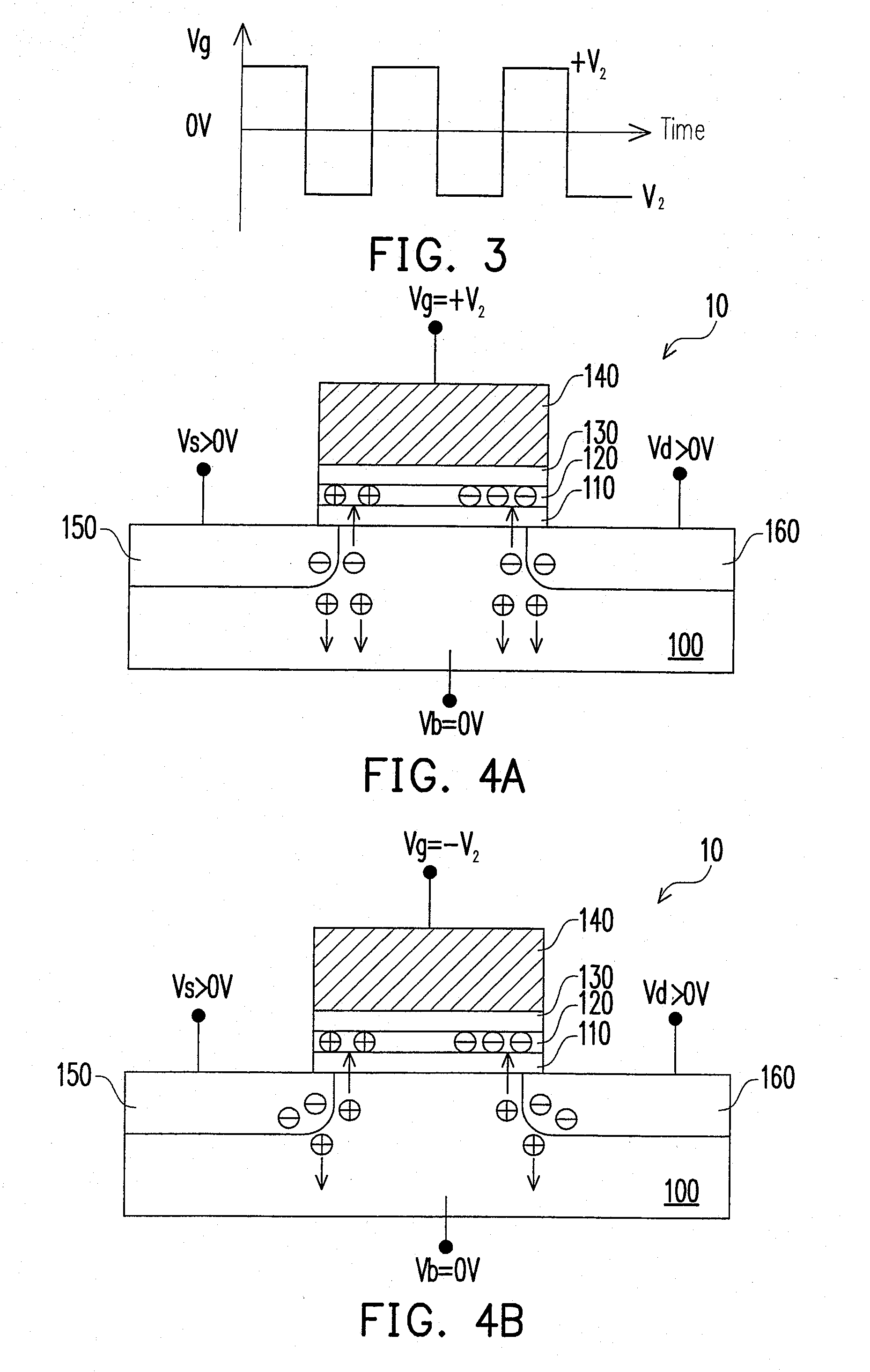
[0033]FIGS. 3, 4A and 4B depict a non-volatile memory and a reset method of the non-volatile memory according to the second embodiment of this invention, wherein the non-volatile memory is reset to...


PUM


Abstract

A non-volatile memory includes a plurality of cells on a substrate of a first conductivity type, each cell including a portion of the substrate, a control gate, a charge-storing layer between the portion of the substrate and the control gate, and two S / D regions of a second conductivity type in the portion of the substrate. A circuit provides a first voltage to the substrate and a second voltage to both S / D regions of each cell, wherein the difference between the first and second voltages is sufficient to cause band-to-band tunneling hot holes. The circuit also provides a voltage to the control gate and the period of applying the voltages are controlled such that the threshold voltages of all the cells converge in a tolerable range.

Description

CROSS-REFERENCE TO RELATED APPLICATION[0001]This application is a continuation of and claims priority benefit of an application Ser. No. 11 / 620,450, filed on Jan. 5, 2007. The entirety of the above-mentioned patent application is hereby incorporated by reference herein and made a part of specification.BACKGROUND OF THE INVENTION[0002]1. Field of the Invention[0003]The present invention relates to a semiconductor device, and more particularly to a non-volatile memory, wherein the threshold voltage of the non-volatile memory converges in a tolerable range of predetermined threshold voltages.[0004]2. Description of Related Art[0005]Electrically erasable programmable non-volatile memory, such as flash memory, is operated usually based on electron injection into a charge-storing layer and electron removal from the same. The electron removal operation is carried out by, for example, ejecting the electrons out of the charge-storing layer or injecting electric holes into the charge-storing ...

Claims


Application Information

Patent Timeline
Patent Type & Authority Applications(United States)
IPC IPC(8): G11C16/04G11C11/34G11C16/06
CPCG11C16/3404
Inventor KUO, MING-CHANG
Owner MACRONIX INT CO LTD
Why Eureka
Try Eureka