
Trench moseft with trench gates underneath contact areas of ESD diode for prevention of gate and source shortate

a technology of trench gates and moseft, which is applied in the field of cell structure, device configuration and fabrication process of moseft transistors, can solve the problems of permanent damage, dangerous conditions of dmos devices, and conventional technologies still have technical difficulties in dealing with electrostatic discharge (esd), so as to avoid esd shorting

Inactive Publication Date: 2009-08-27
FORCE MOS TECH CO LTD
View PDF4 Cites 17 Cited by
  • Summary
  • Abstract
  • Description
  • Claims
  • Application Information

AI Technical Summary

Benefits of technology

[0009]The present invention provides a trench DMOS transistor having overvoltage protection and the ability to avoid ESD shorting with source when trench contacts are applied.

Problems solved by technology

Conventional technologies still have technical difficulties in dealing with the electrostatic discharge (ESD) problems in designing, manufacturing and implementing the semiconductor power devices.
The high electric field induced by the bias voltage when imposed on a relatively thin layer of gate dielectric layer often leads to hazardous conditions to the DMOS device.
A permanent damage is thus introduced into a system implemented with the power semiconductor device.
The reliability of system performance and operations suffer due this ESD problem.
This problem is particularly pronounced in high voltage DMOS devices.
FIG. 3 shows the disadvantage of the DMOS structure of FIG. 2 when trench contacts into epitaxial layer are applied.
One problem with the device shown in the previously mentioned patent is that if trench contacts are applied for source and gate which requires additional Si trench etch, the prior art shown in FIG. 2 will encounter the ESD diode shorting with body-source, causing low yield and reliability issues, as shown in FIG. 3.
The shortage is resulted from etch through ESD diode poly and thin oxide underneath mentioned above, which will lead to a permanent damage to the device.

Method used


Image

  • Trench moseft with trench gates underneath contact areas of ESD diode for prevention of gate and source shortate
  • Trench moseft with trench gates underneath contact areas of ESD diode for prevention of gate and source shortate
  • Trench moseft with trench gates underneath contact areas of ESD diode for prevention of gate and source shortate

Examples


Embodiment Construction

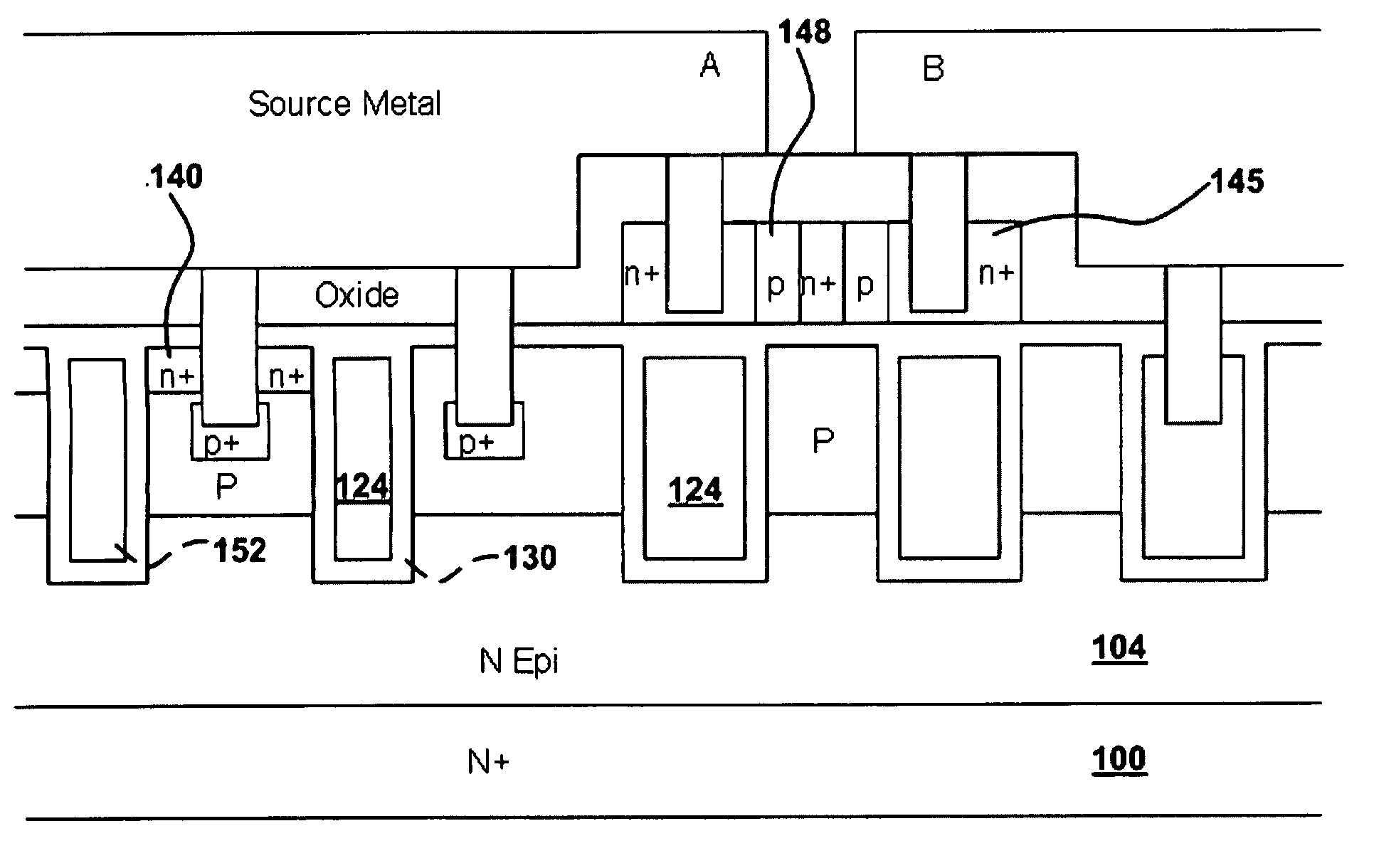
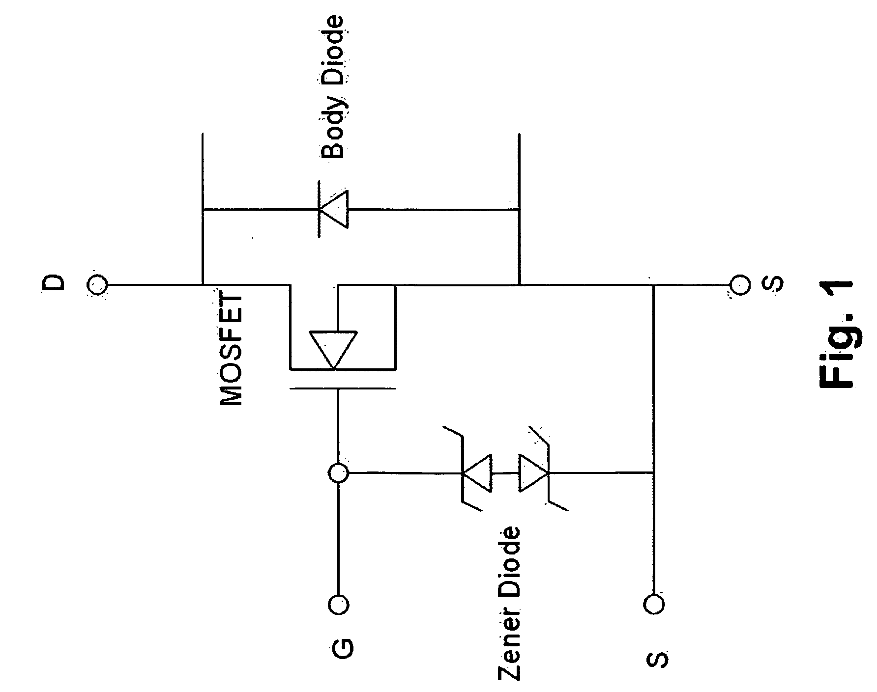
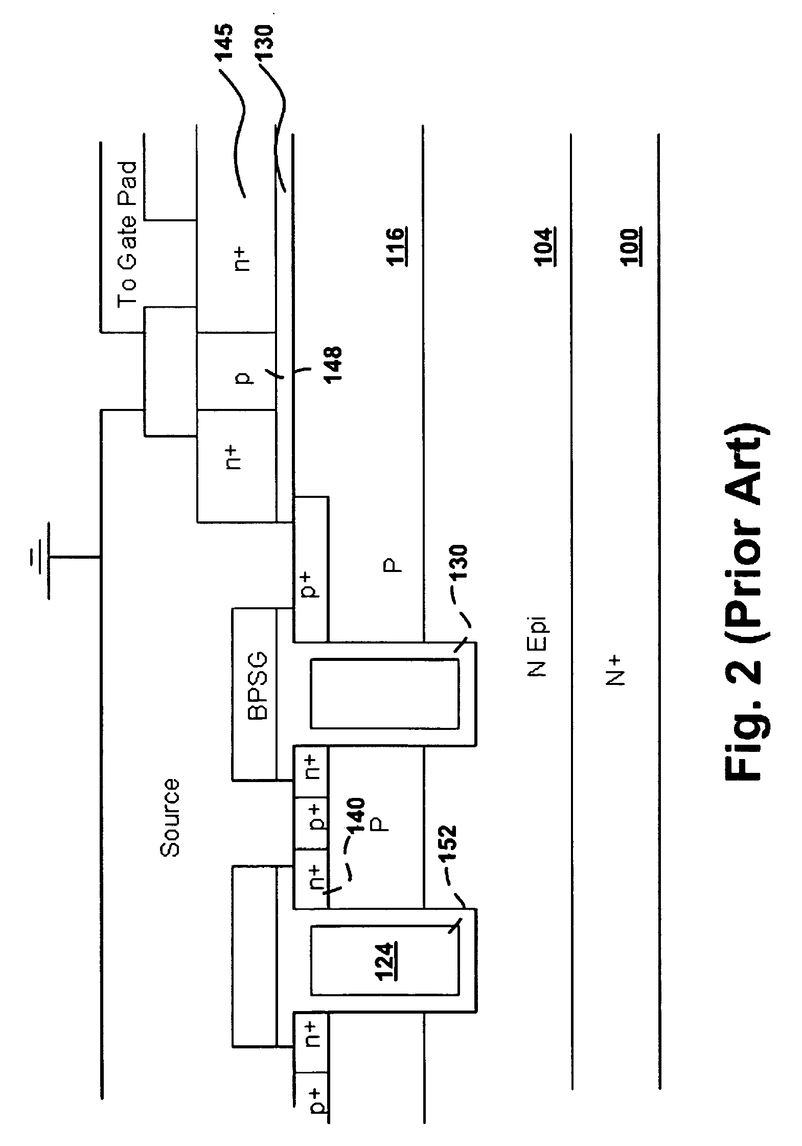
[0023]FIG. 4 illustrates the DMOS structure of this invention in cross-section. In FIG. 4, the ESD protection diode comprises cathodes 145 and anode 148. Trench gates are formed underneath contact areas of the ESD protection diode in order to resolve the problems discussed above. Besides these, the structure shown in FIG. 4 is advantageous because the source region 140 of the DMOS transistor and n+ cathode regions 145 of the Zener diode can be formed in the same mask and implantation steps, and all the trenches gate can be formed in the same mask and in the same step.

[0024]FIG. 5 illustrates the function of this invention when trenches are overetched. The ESD diode does not short to body-source as result of the trench gate underneath the contact area as buffer layer. The ESD diode will touch to the trench gates underneath without shorting source area.

[0025]FIGS. 6A-6G show a series of exemplary steps that are performed to form the inventive trench DMOS devices. In FIG. 6A, an N− dop...


PUM


Abstract

A trench DMOS transistor having overvoltage protection and prevention for shortage between gate and source when contact trenches are applied includes a substrate of a first conductivity type and a body region of a second conductivity type formed over the substrate. Trench gates extend through the body region and the substrate. An insulating oxide layer lines the trench and overlies the body region. A conductive electrode is deposited in the trench so that it overlies the insulating layer. A source region of the first conductivity type is formed in the body region adjacent to the trench. An undoped polysilicon layer overlies a portion of the insulating layer defining the Zener diode region. A plurality of cathode regions of the first conductivity type is formed in undoped polysilicon layer. At least one anode region is in contact with adjacent ones of the plurality of cathode regions. Trench gates underneath the Zener diode act as the buffer layer for prevention of shortage between gate and source.

Description

FIELD OF THE INVENTION[0001]This invention relates generally to the cell structure, device configuration and fabrication process of MOSFET transistors. More particularly, this invention relates to a novel and improved cell configuration and processes to manufacture DMOS transistors with electrostatic discharge (ESD) protection having the characteristics of preventing for gate and source shortage.BACKGROUND[0002]Conventional technologies still have technical difficulties in dealing with the electrostatic discharge (ESD) problems in designing, manufacturing and implementing the semiconductor power devices. Specially, the high voltage transient signal from static discharge in a DMOS device can impose a voltage bias higher than 10,000 volts. The high electric field induced by the bias voltage when imposed on a relatively thin layer of gate dielectric layer often leads to hazardous conditions to the DMOS device. The thin layer of gate dielectric is most commonly implemented as an oxide l...

Claims


Application Information

Patent Timeline
Patent Type & Authority Applications(United States)
IPC IPC(8): H01L27/06
CPCH01L27/0255H01L27/0629H01L29/41766H01L29/7813H01L29/66727H01L29/66734H01L29/7808H01L29/4236
Inventor HSIEH, FU-YUAN
Owner FORCE MOS TECH CO LTD
Learn More