Sliced electromagnetic cage for inductors

a technology of electromagnetic cage and inductors, which is applied in the field of integrated circuits, can solve the problems of insufficient knowledge of engineers, inability to meet spacing requirements, and degradation of integrated circuit performance, and achieve the effect of compact layout placemen

Active Publication Date: 2009-07-16
MEDIATEK INC
View PDF10 Cites 10 Cited by
  • Summary
  • Abstract
  • Description
  • Claims
  • Application Information

AI Technical Summary

Benefits of technology

[0008]A system and method in accordance with the present invention adds metal walls on the edge of a sliced shield. The walls block the electromagnetic wave from coupling to other parts of the circuit from a sideways direction. The use of this structure allows for more compact layout placement with insignificant degradation.

Problems solved by technology

But even with the shielding 14 underneath the inductor, routing traces nearby (like power lines 16, and signal traces 20) still degrade the performance of the integrated circuit.
Engineers don't know ahead of time which device or devices is going to be next to the inductor, so they leave space to make sure the devices are completely separated as much as possible.
It is especially critical because layout engineers do not necessarily know which device or devices may be next to others.
As integrated circuits become smaller this spacing requirements becomes unacceptable.
In addition, even when the inductor is separated from the other parts of the integrated circuit in this manner, there is still the possibility of eddy current and direct coupling from the lossy substrate and metal traces nearby, which may come in from sideways, beneath, or on top.
Otherwise, the quality factor of planar inductor suffers from electromagnetic losses due to eddy current and direct coupling from lossy substrate and metal traces nearby.
Thus the inductor Q factor has degradation due to compact IC layout.

Method used


Image

  • Sliced electromagnetic cage for inductors
  • Sliced electromagnetic cage for inductors
  • Sliced electromagnetic cage for inductors

Examples


Embodiment Construction

[0014]The present invention relates generally to integrated circuits and more specifically to minimizing losses when utilizing devices in such circuits. The following description is presented to enable one of ordinary skill in the art to make and use the invention and is provided in the context of a patent application and its requirements. Various modifications to the preferred embodiment and the generic principles and features described herein will be readily apparent to those skilled in the art. Thus, the present invention is not intended to be limited to the embodiment shown but is to be accorded the widest scope consistent with the principles and features described herein.

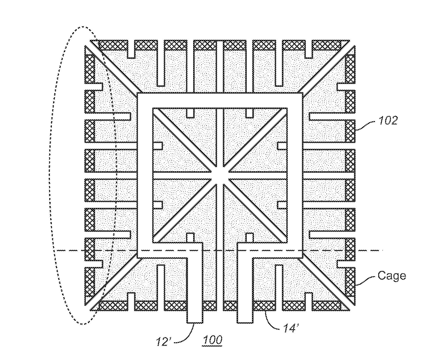
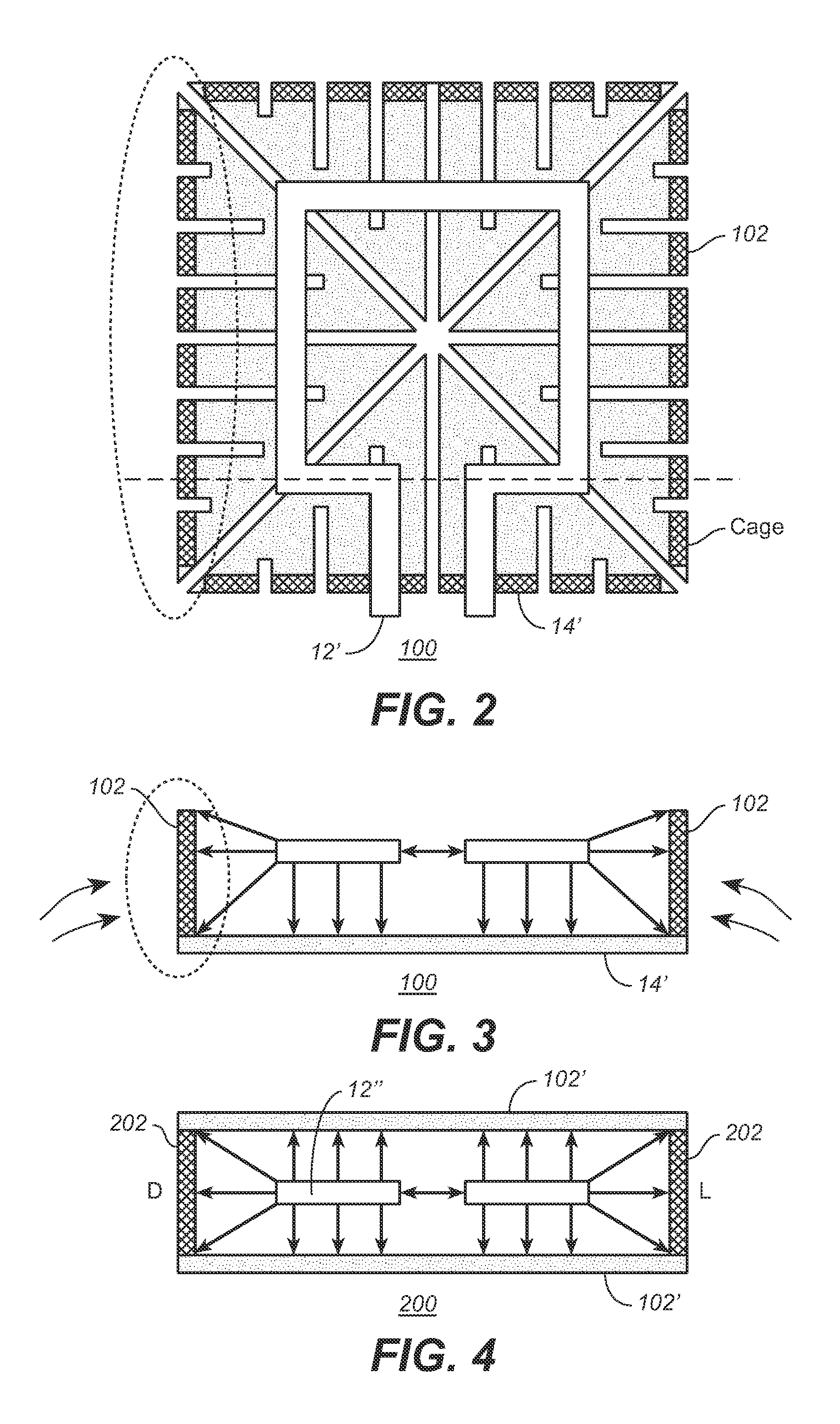
[0015]In a system and method in accordance with the present invention the electromagnetic (EM) wave seen by a lossy wafer substrate and the nearby routing is blocked more completely than with conventional systems. FIG. 2 shows a first embodiment of a shielding system 100 in accordance with the present invention...


PUM


Abstract

A system within a circuit is disclosed. The system comprises a first shield and a device above the first shield. The system also includes a plurality of conductive walls coupled to and extending from the first shield to block electromagnetic (EM) waves to other parts of the circuit. A system and method in accordance with the present invention adds metal walls on the edge of a sliced shield. The walls block the electromagnetic wave from coupling to other parts of the circuit from a sideways direction. The use of this structure allows for more compact layout placement with insignificant degradation.

Description

FIELD OF THE INVENTION[0001]The present invention relates generally to integrated circuits and more specifically to minimizing losses when utilizing inductors in such circuits.BACKGROUND OF THE INVENTION[0002]Inductors are utilized extensively in a variety of integrated circuits. FIGS. 1A and 1B illustrate a top and side view of an inductor 12 with metal shielding 14 underneath on top of a substrate 10. Shielding 14 is added under the inductor 12 to move other circuits farther away from the inductor and also to prevent eddy currents and couplings to external circuits and lines. But even with the shielding 14 underneath the inductor, routing traces nearby (like power lines 16, and signal traces 20) still degrade the performance of the integrated circuit. At the present time, layout engineers use spacing to separate the inductor from the other parts of the integrated circuit or device from another. Engineers don't know ahead of time which device or devices is going to be next to the i...

Claims


Application Information

Patent Timeline
Patent Type & Authority Applications(United States)
IPC IPC(8): H05K9/00H05K1/16
CPCH01F17/0006H01F27/367H01F2017/008H01L23/552H01L2924/0002H01L23/645H01L2924/00H01F27/36H01F27/363
Inventor LU, ERIC CHIYUAN
Owner MEDIATEK INC
Why Eureka
Try Eureka