Semiconductor device and method of manufacturing the semiconductor device
a semiconductor and semiconductor technology, applied in the direction of fixed capacitor details, stacked capacitors, fixed capacitors, etc., can solve the problems of becoming impossible to reliably form the mim capacitance element, becoming impossible to obtain targeted high-frequency characteristics, etc., to achieve small parasitic resistance, small parasitic capacitance, and superior high-frequency characteristics
- Summary
- Abstract
- Description
- Claims
- Application Information
AI Technical Summary
Benefits of technology
Problems solved by technology
Method used
Image
Examples
embodiment 1
Preferred Embodiment 1
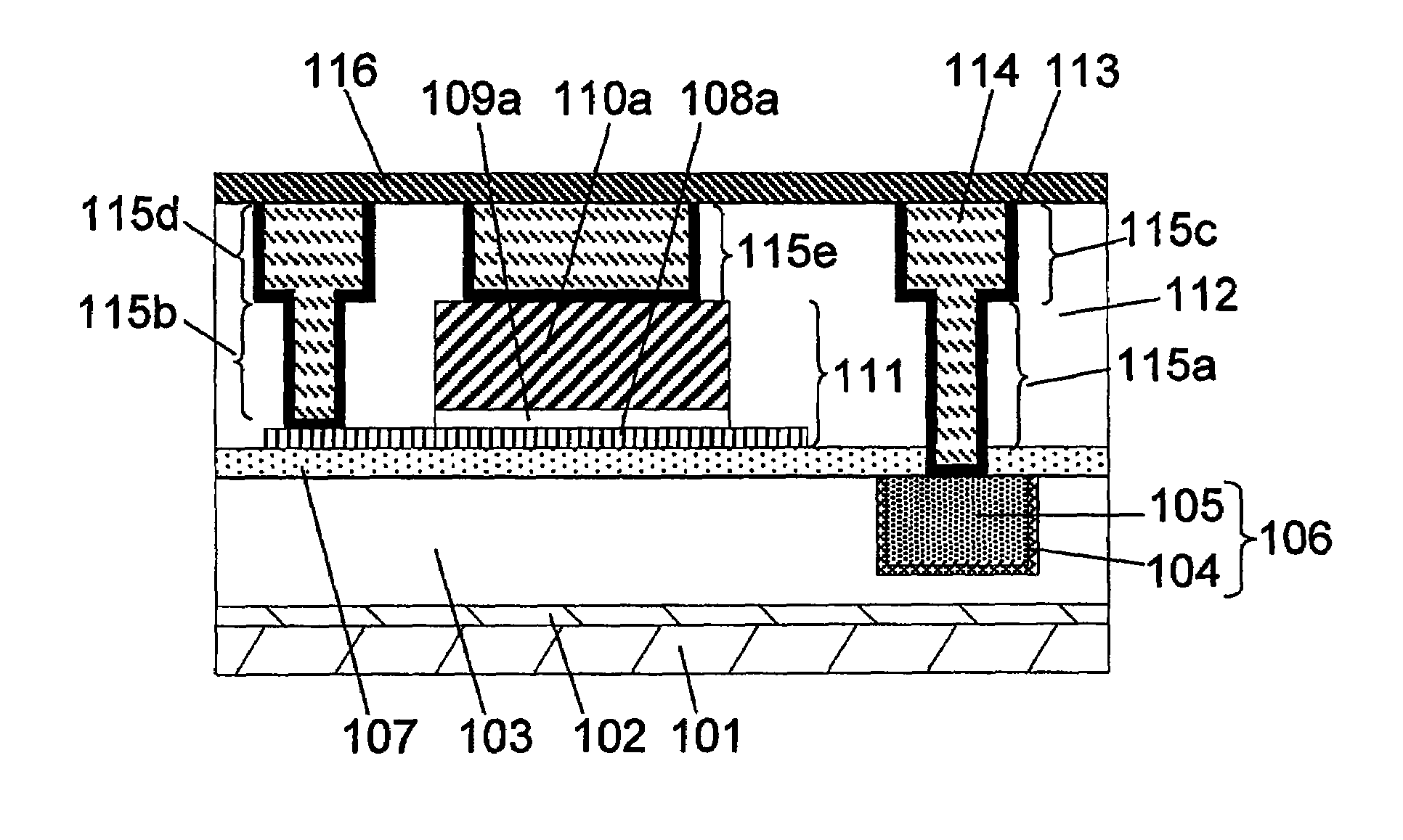
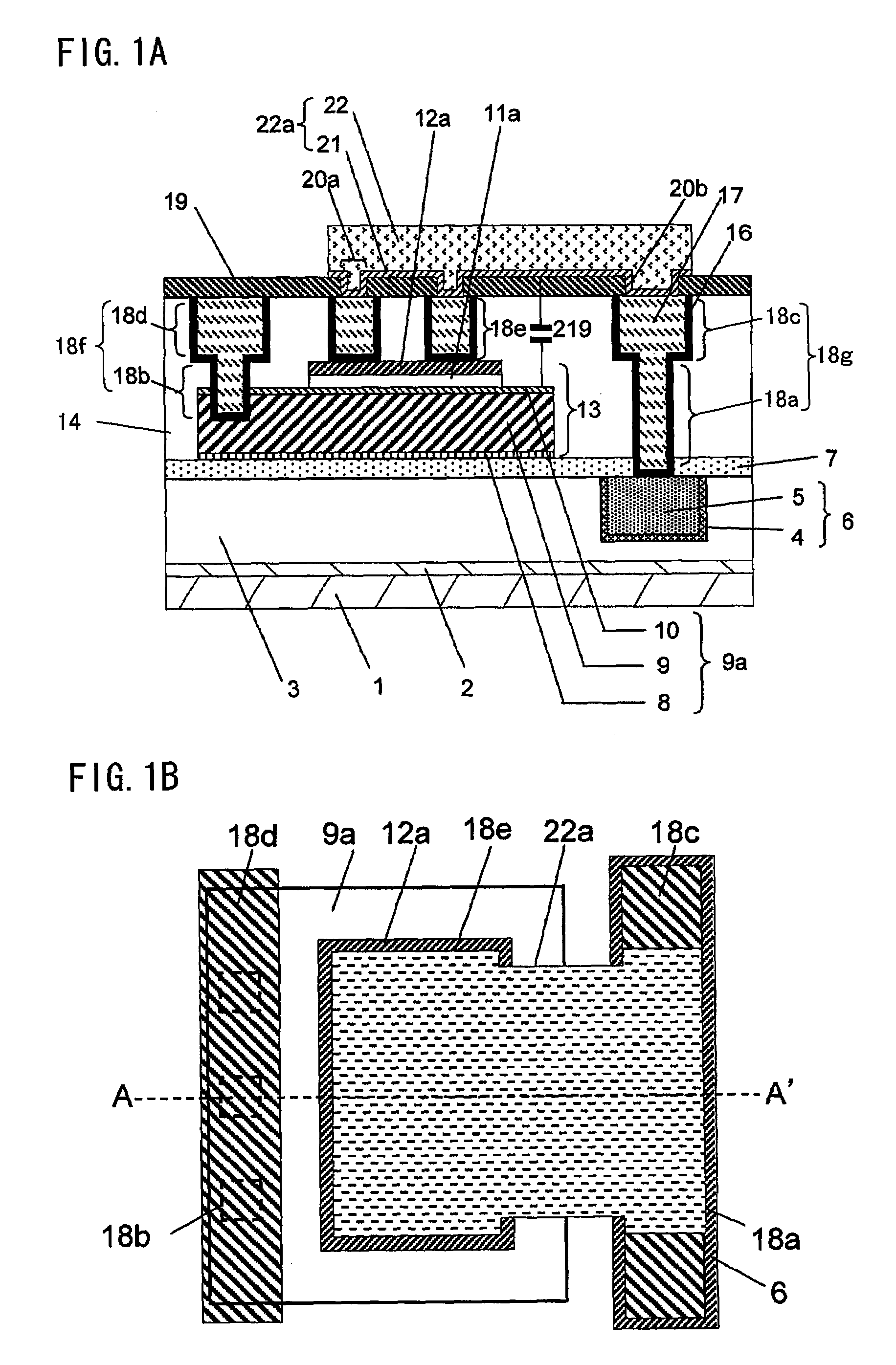
[0054]FIGS. 1A and 1B are respectively a sectional view and a planar view illustrating a semiconductor device according to a preferred embodiment 1 of the present invention, wherein an MIM capacitance element and wiring layers (upper wiring layer and lower wiring layer) are illustrated. As illustrated in FIG. 1A, an insulating isolation layer 2 is formed on a semiconductor substrate 1, and a first insulation film 3 is further formed on the insulating isolation layer 2. A lower wiring layer 6 is embedded in an upper section (surface portion) of the first insulation film 3. A Cu layer 5 and a first barrier metal film 4 (TaN film) constitute the lower wiring layer 6. A barrier insulation film 7 is formed on the first insulation film 3 and the lower wiring layer 6. The barrier insulation film 7, which is made of a SiN film (thickness is approximately 200 nm), is provided for the diffusion of Cu and the prevention of oxidation. An MIM capacitance element 13 is forme...
embodiment 2
Preferred Embodiment 2
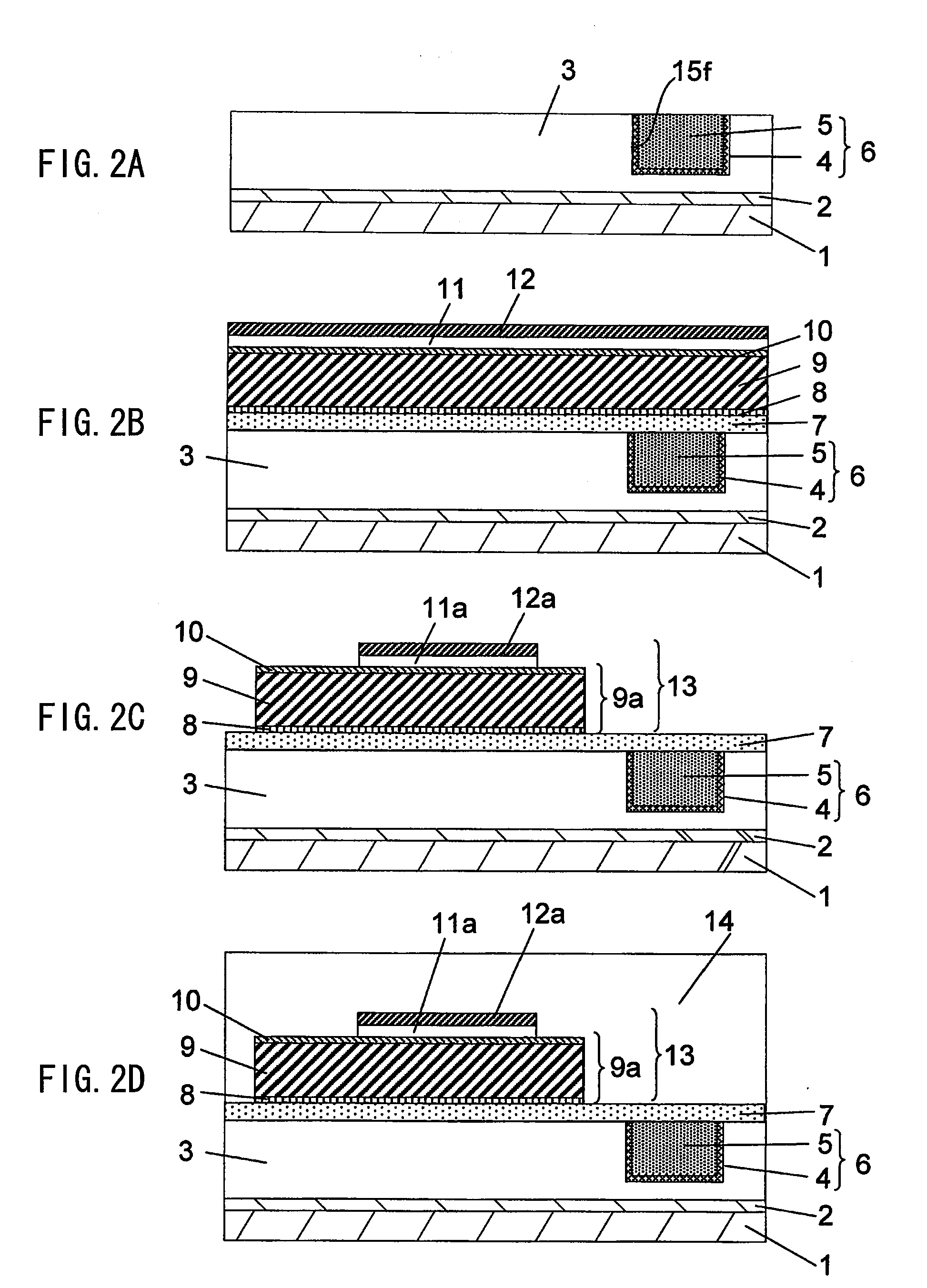
[0061]FIGS. 2A-2D, FIGS. 3A-3C and FIGS. 4A and 4B are sectional views illustrating steps in semiconductor device manufacturing methods according to a preferred embodiment 2 of the present invention. These drawings particularly illustrate the method of manufacturing the semiconductor device including the MIM capacitance element as illustrated in FIGS. 1 and 2.
[0062]As illustrated in FIG. 2A, first, a first insulation film 3 is formed on an insulating isolation layer 2 formed on a semiconductor substrate 1. Then, a lower wiring groove 15f is formed in the first insulation film 3, and thereafter, a TaN film is deposited in the thickness of approximately 20 nm on a surface of the lower wiring groove 15f by means of sputtering, so that a first barrier metal film 4 is formed. The first barrier metal film 4 is provided for the diffusion of Cu and the prevention of oxidation. A Cu film having the thickness of approximately 100 nm is deposited on the first barrier meta...
PUM
 Abstract
Description
Claims
Application Information
 - R&D
- Intellectual Property
- Life Sciences
- Materials
- Tech Scout
- Unparalleled Data Quality
- Higher Quality Content
- 60% Fewer Hallucinations
Browse by: Latest US Patents, China's latest patents, Technical Efficacy Thesaurus, Application Domain, Technology Topic, Popular Technical Reports.
© 2025 PatSnap. All rights reserved.Legal|Privacy policy|Modern Slavery Act Transparency Statement|Sitemap|About US| Contact US: help@patsnap.com


