
Semiconductor integrated circuit

a technology of integrated circuits and semiconductors, applied in the direction of demodulation, electrical equipment, transmission, etc., can solve the problems of large chip size and inability to make smaller chips, and achieve the effect of reducing the number of downconverting signals, and reducing the number of system components

Inactive Publication Date: 2009-06-04
RENESAS ELECTRONICS CORP
View PDF16 Cites 23 Cited by
  • Summary
  • Abstract
  • Description
  • Claims
  • Application Information

AI Technical Summary

Benefits of technology

This approach reduces the capacitance of the filter, enabling a more compact chip design, reducing the number of external components, and maintaining the desired noise and signal characteristics, thus facilitating smaller system size and lower production costs.

Problems solved by technology

This results in a larger chip size, so that the chip cannot be made smaller.

Method used


Image

  • Semiconductor integrated circuit
  • Semiconductor integrated circuit
  • Semiconductor integrated circuit

Examples


second embodiment

[0052]FIG. 4 shows an example of configuration of a mixer circuit according to a

[0053]In this embodiment, a current mirror circuit including PMOSFETs is used as the current sources CS1 and CS2. The drain terminals of the PMOSFETs Q2 and Q3 included in the current mirror circuit are connected to the collectors of the lower stage differential transistors Q12 and Q11 of the mixer circuit, respectively, so that the currents from the PMOSFETs Q2 and Q3 are directly applied to the lower stage differential transistors Q12 and Q11. Using this configuration causes no problem circuitwise, since the impedances of the PMOSFETs included in the current mirror circuit are adequately higher than the impedances of the collector connection nodes of the lower stage differential transistors Q12 and Q11.

third embodiment

[0054]FIG. 5 shows an example of configuration of a mixer circuit according to a

[0055]In this embodiment, resistors R1 and R2 connected between a supply voltage terminal and the collectors of the lower stage differential transistors Q11 and Q12, respectively, are used as the current sources CS1 and CS2 for current application. A suitable resistance range for the resistors R1 and R2 is from several hundred ohms to several kilo-ohms. When the resistors R1 and R2 each having a resistance in the range of several hundred ohms to several kilo-ohms are connected between the supply voltage terminal and the collectors of the lower stage differential transistors Q11 and Q12, respectively, the resistors R1 and R2 are higher in impedance than the collector connection nodes of the lower stage differential transistors Q11 and Q12, so that no problem is caused circuitwise.

[0056]When PMOFETs are used in a mixer circuit, they generate larger noise than resistors. In terms of the noise characteristic...


PUM


Abstract

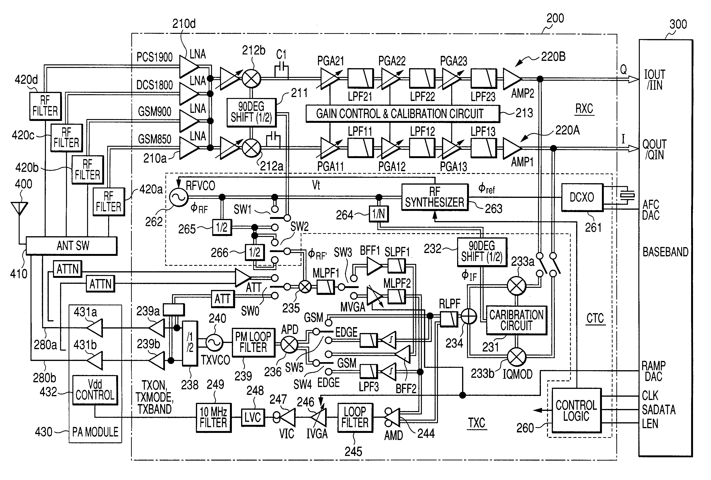
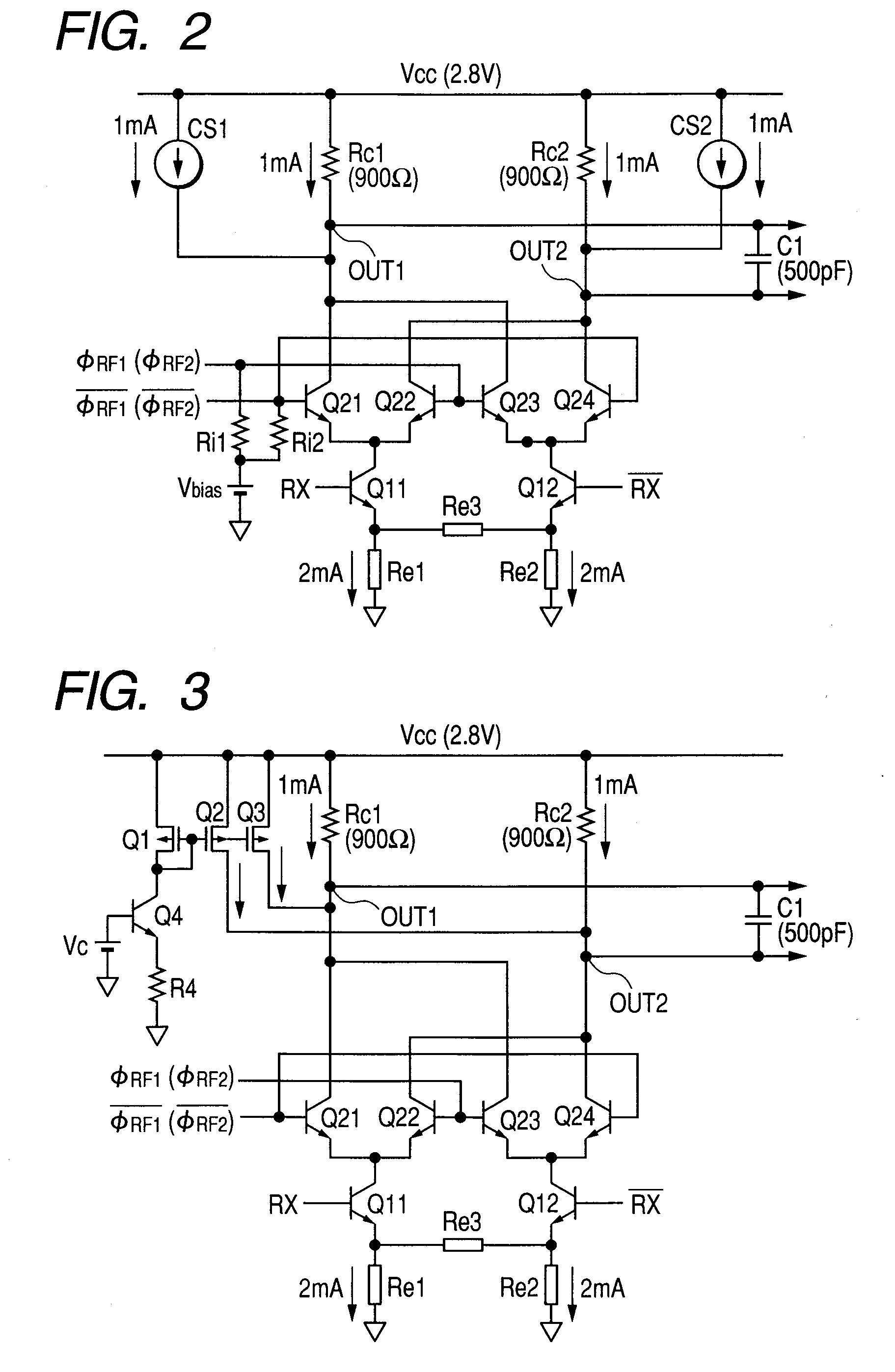
In a communication semiconductor integrated circuit, a capacitance included in a filter on the output side of a mixer circuit is reduced without requiring the cutoff frequency of the filter to be changed. A Gilbert cell circuit is used as a mixer circuit which combines, for downconversion, a reception signal and a local oscillator signal. A low-pass filter for removing unwanted waves from output is composed of load resistors of upper stage differential transistors and a capacitive element provided between differential output terminals. The resistances of the load resistors are increased, and a current circuit for applying a current to emitters or collectors of the upper stage differential transistors is provided, so that a current to make up for a decrease in current amount attributable to the increase in load resistance can be applied from the current circuit to lower stage differential transistors.

Description

[0001]This application is a continuation application of U.S. application Ser. No. 11 / 387,897, filed Mar. 24, 2006, now allowed.CROSS-REFERENCE TO RELATED APPLICATION[0002]The present application claims priority from Japanese patent application No. 2005-093840 filed on Mar. 29, 2005, the content of which is hereby incorporated by reference into this application.BACKGROUND OF THE INVENTION[0003]The present invention relates to a technique effective in forming on an IC chip a filter with a reduced capacitance to be provided on the output side of a direct downconversion mixer which, for frequency conversion, combines a reception signal and an oscillator signal of a prescribed frequency. More particularly, the invention relates to a technique which can be effectively applied, for example, to a semiconductor integrated circuit (radio frequency IC) for processing radio frequency signals.[0004]In a radio communication system such as a portable telephone, a radio frequency IC (RF IC) incorpo...

Claims


Application Information

Patent Timeline
Patent Type & Authority Applications(United States)
IPC IPC(8): H04B1/28
CPCH03D7/1433H04B1/28H03D2200/0033H03D7/1458H03D2200/0025H03D7/145
Inventor YOSHIZAKI, YASUNOBUWAKUDA, TETSUYA
Owner RENESAS ELECTRONICS CORP
Learn More