Integrated circuit package having reversible ESD protection

a technology of integrated circuits and integrated circuits, which is applied in the direction of semiconductor/solid-state device testing/measurement, semiconductor/solid-state device details, instruments, etc., can solve the problems of inability to perform esd testing with the bga package mounted to the circuit board, circuit board may not be available, and inability to perform esd testing

Inactive Publication Date: 2009-05-28
AVAGO TECH WIRELESS IP SINGAPORE PTE
View PDF5 Cites 11 Cited by
  • Summary
  • Abstract
  • Description
  • Claims
  • Application Information

AI Technical Summary

Problems solved by technology

However, in some situations, it may not be practical to perform the ESD testing with the BGA package mounted to the circuit board.
For example, the circuit board may not yet be designed, the circuit board may not be available to the BGA package manufacturer, and / or further reasons may make such ESD testing impractical.
Thus, in some situations, it may not be possible or practical to perform ESD testing of a BGA package in a manner that verifies ESD protection for the package in its actual operating environment.

Method used


Image

  • Integrated circuit package having reversible ESD protection
  • Integrated circuit package having reversible ESD protection
  • Integrated circuit package having reversible ESD protection

Examples


example integrated

Circuit Packages

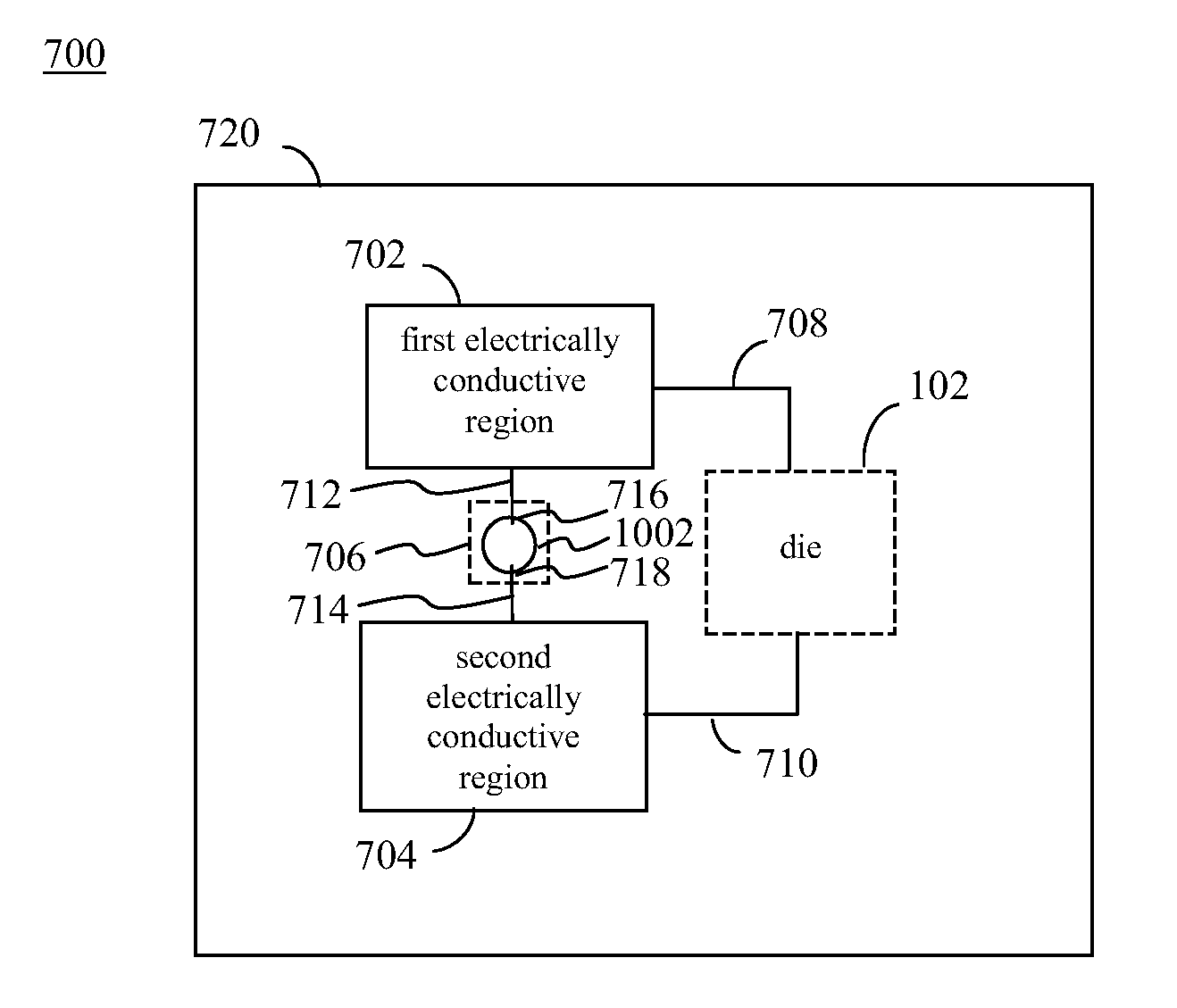
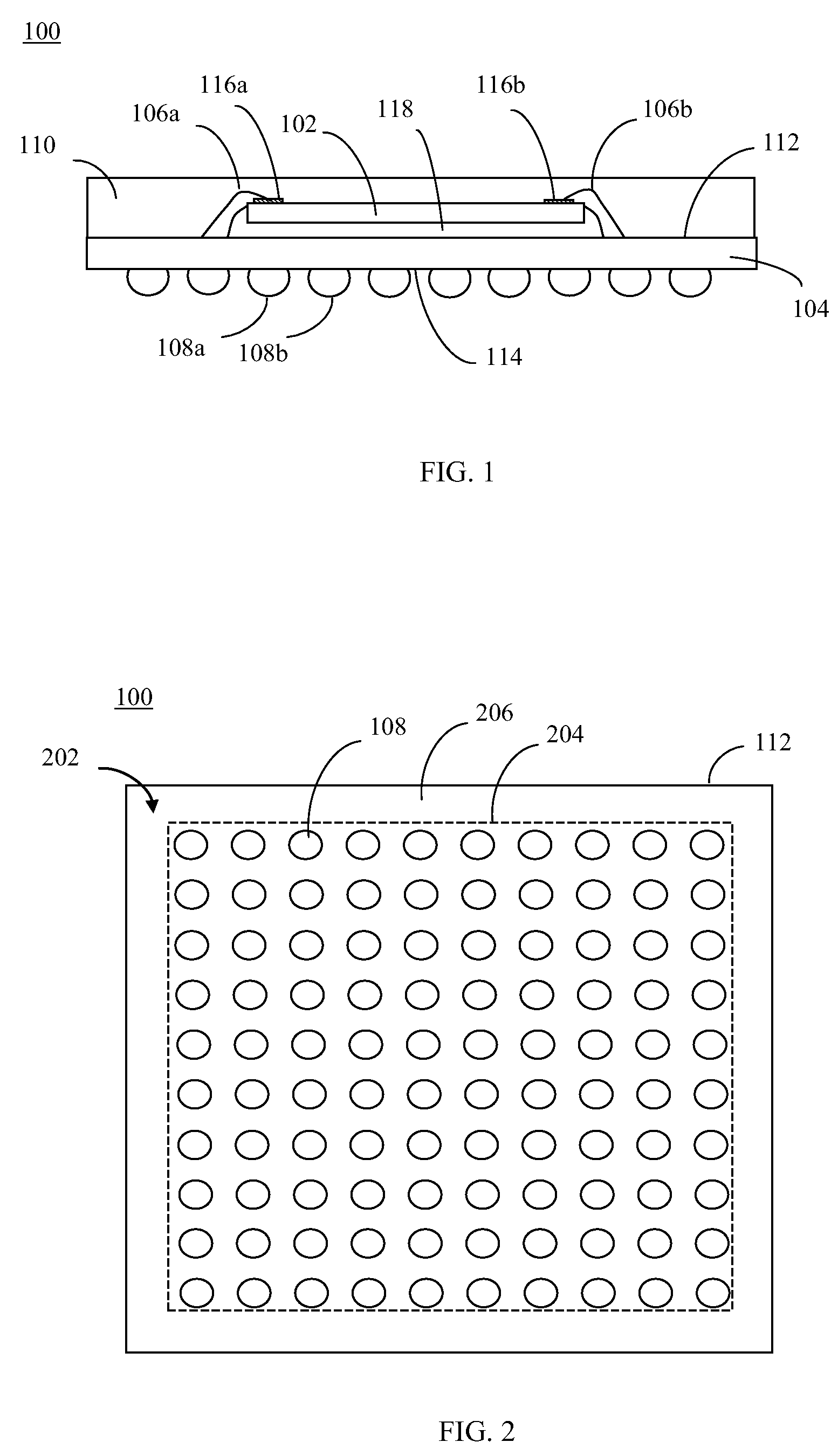
[0026]Embodiments of the present invention are applicable to a variety of types of integrated circuit packages, including ball grid array (BGA) packages. FIG. 1 shows a cross-sectional view of an example BGA package 100. BGA package 100 may be a plastic BGA (PBGA) package, a flex BGA package, a ceramic BGA package, a fine pitch BGA (FPBGA or FBGA) package, or other type of BGA package. BGA package 100 includes an integrated circuit die / chip 102, a substrate 104, bond wires (also known as “wire bonds”) 106, a plurality of solder balls 108, and an encapsulating material 110. Substrate 104 has a first (e.g., top) surface 112 that is opposed to a second (e.g., bottom) surface 114 of substrate 104. As shown in FIG. 1, die 102 is mounted to first surface 112 of substrate 104. Die 102 may be mounted to substrate 104 using an adhesive material 118.

[0027]As shown in FIG. 1, a plurality of bond wires 106 are coupled between terminals 116 of die 102 and electrically conductive ...

example embodiments

[0035]The example embodiments described herein are provided for illustrative purposes, and are not limiting. Although described with reference to BGA packages, the examples described herein may be adapted to various types of integrated circuit packages, including other land grid array (LGA) package types, pin grid array (PGA) packages, and further types of integrated circuit packages having conductive elements such as pads / balls / pins in an array on a surface. Furthermore, additional structural and operational embodiments, including modifications / alterations, will become apparent to persons skilled in the relevant art(s) from the teachings herein.

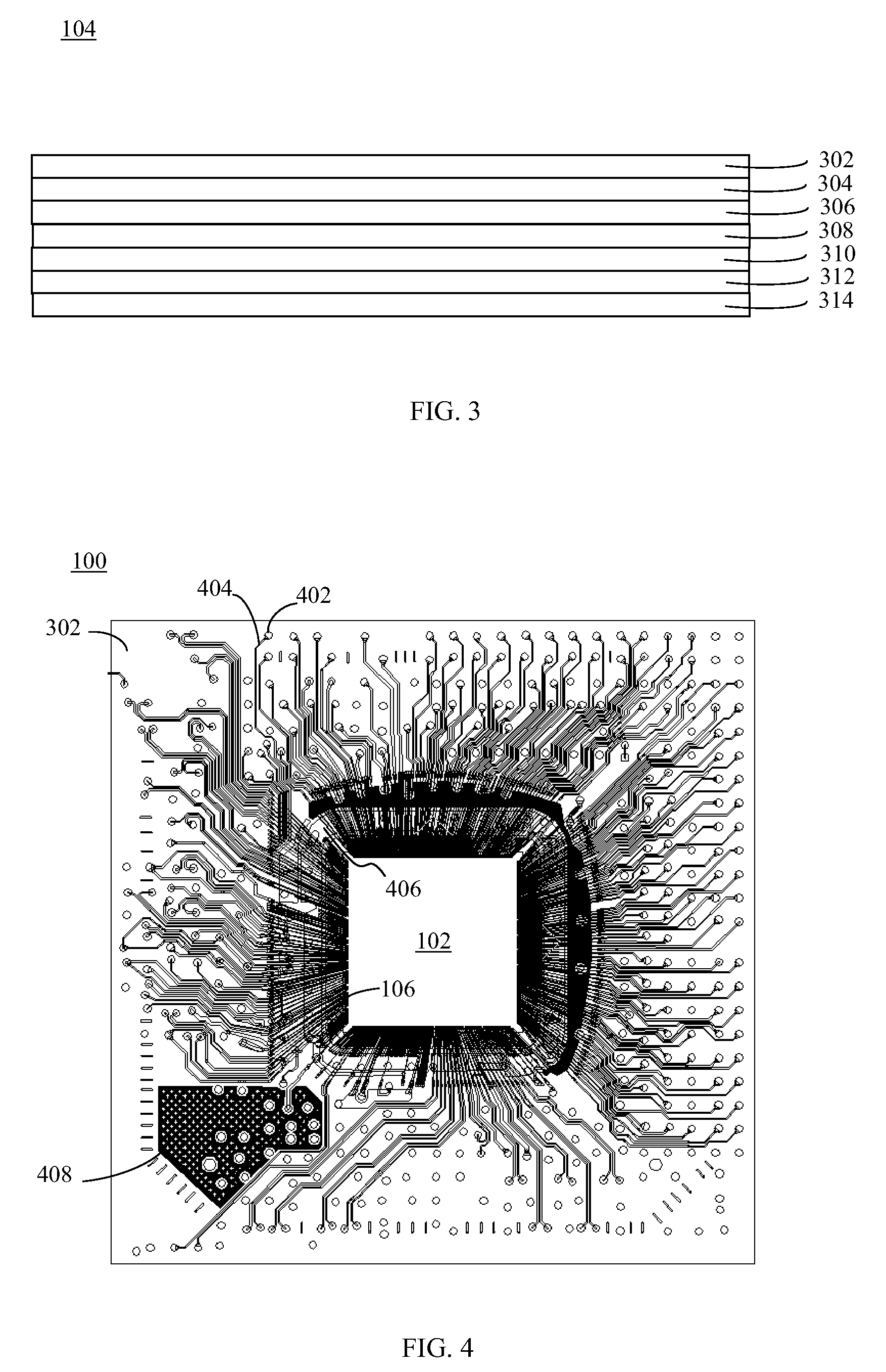
[0036]Embodiments of the present invention may be implemented in substrates of integrated circuit packages, such as substrate 104 of BGA package 100. FIG. 3 shows a side cross-sectional view of an example of substrate 104. As shown in FIG. 3, substrate 104 includes a first (top) layer 302, a second layer 304, a third layer 306, a fourth laye...


PUM


Abstract

Methods, systems, and apparatuses are provided for integrated circuit packages and for enabling electrostatic discharge (ESD) testing of the same. A package includes an integrated circuit chip, a substrate, a first electrically conductive trace, and a second electrically conductive trace. The substrate includes a first electrically conductive region and a second electrically conductive region. The first region is coupled to a first ground signal of the chip, and the second region is coupled to a second ground signal of the chip. The first trace is coupled to the first region and the second trace is coupled to the second region. A portion of the first trace is proximate to a portion of the second trace. An electrically conductive material may be deposited to electrically couple the first and second traces to enable ESD protection testing of the package.

Description

BACKGROUND OF THE INVENTION[0001]1. Field of the Invention[0002]The present invention relates to integrated circuit packaging technology, and more particularly, to electrostatic discharge protection for integrated circuits.[0003]2. Background Art[0004]Integrated circuit (IC) chips or dies from semiconductor wafers are typically interfaced with other circuits using a package that can be attached to a printed circuit board (PCB). One such type of IC die package is a ball grid array (BGA) package. BGA packages provide for smaller footprints than many other package solutions available today. A BGA package has an array of solder ball pads located on a bottom external surface of a package substrate. Solder balls are attached to the solder ball pads. The solder balls are reflowed to attach the package to the PCB.[0005]Millions of BGA packages are manufactured each year for implementation in electronic devices according to increasingly finer fabrication technologies, including 90 nm and 65 ...

Claims


Application Information

Patent Timeline
Patent Type & Authority Applications(United States)
IPC IPC(8): G01R31/26H01L23/58H01L21/58
CPCG01R31/002H01L23/49838H01L23/60H01L2924/01087H01L2924/01079H01L2924/15311H01L24/48H01L2224/48227H01L2924/14H01L2924/181H01L2224/73265H01L2224/45124H01L2224/45139H01L2224/45147H01L2924/00014H01L2224/45144H01L24/45H01L2924/00H01L2924/00012H01L2224/45015H01L2924/207
Inventor LAW, EDMUND
Owner AVAGO TECH WIRELESS IP SINGAPORE PTE
Why Eureka
Try Eureka