Stacked package module and method for fabricating the same
a technology of stacked package modules and conductive pads, which is applied in the manufacture of printed circuits, printed circuit aspects, basic electric elements, etc., can solve the problems of reduced minimum sizes of solder balls and conductive pads, difficulty in reducing the height of the package module, and significant reduction of the use of solder materials and the pitch. , to achieve the effect of reducing cost, avoiding warpage, and shrinking the pitch of conductive pads
- Summary
- Abstract
- Description
- Claims
- Application Information
AI Technical Summary
Benefits of technology
Problems solved by technology
Method used
Image
Examples
embodiment 1
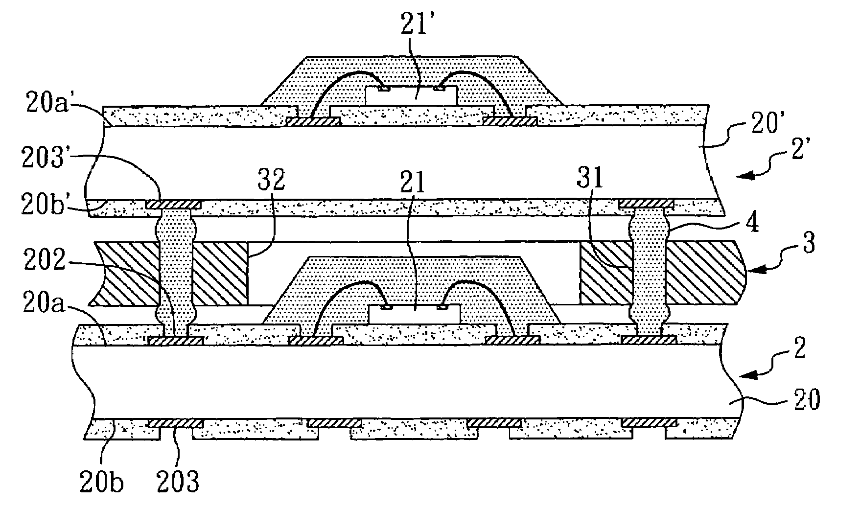
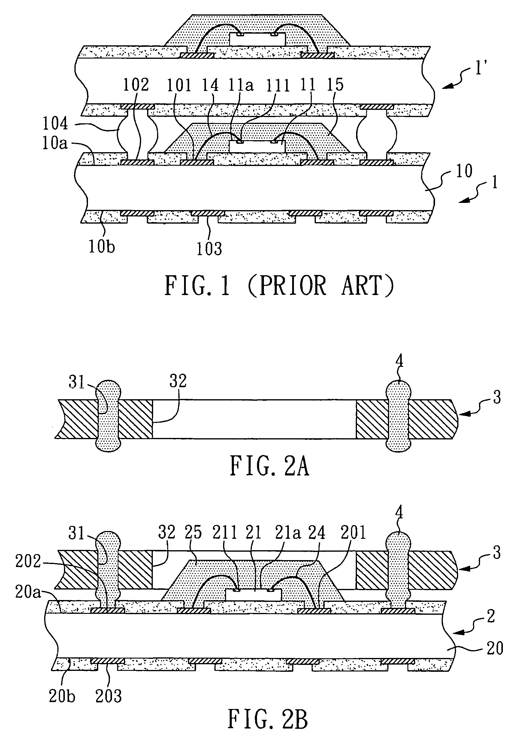
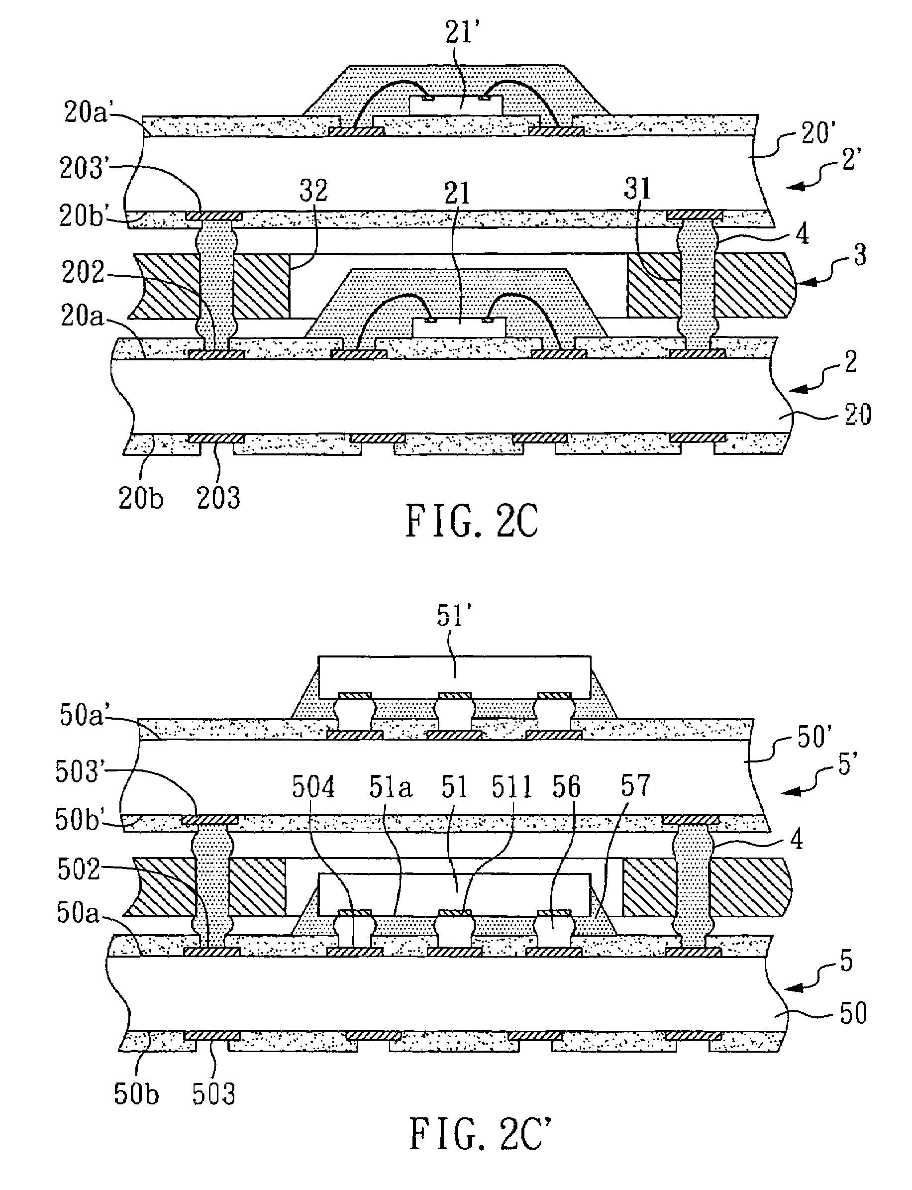
[0022]With reference to FIGS. 2A to 2C, there are shown cross-sectional views for illustrating a method for fabricating a stacked package module according to a preferred embodiment of the present invention.
[0023]As shown in FIG. 2A, a ceramic-surfaced aluminum plate 3 is first provided, which has a plurality of through holes 31 and a first cavity 32. Then, the through holes 31 are filled with a metal paste 4. Herein, the through holes 31 can be filled with the metal paste 4 by printing or dispensing and the material of the metal paste 4 is not limited. In the present embodiment, the metal paste 4 is copper paste with which the through holes 31 are filled by dispensing.
[0024]Subsequently, as shown in FIG. 2B, a first package structure 2 is placed on one surface of the ceramic-surfaced aluminum plate 3. Herein, the first package structure 2 includes a first chip 21 and a first packaging substrate 20. The first chip 21 electrically connects to the first packaging substrate 20 that has ...
embodiment 2
[0028]The present embodiment is the same as Embodiment 1, except that in the present embodiment the second chip 21′ is disposed on the second surface 20b′ of the second packaging substrate 20′, and the ceramic-surfaced aluminum plate 3 further has a second cavity 33 to receive the second chip 21′ as shown in FIG. 3A.
[0029]Also, the present embodiment provides another stacked package module as shown in FIG. 3A′. The structure illustrated in FIG. 3A′ is the same as that of FIG. 3A, except that the first package structure 5 and the second package structure 5′ are flip chip package structures.
embodiment 3
[0030]The present embodiment is the same as Embodiment 2, except that at least one first passive component 23 is disposed on the first surface 20a of the first packaging substrate 20 in the present embodiment, and the ceramic-surfaced aluminum plate 3 further has at least one third cavity 34 to receive the first passive component 23, as shown in FIG. 3B.
[0031]Also, the present embodiment provides another stacked package module as shown in FIG. 3B′. The structure illustrated in FIG. 3B′ is the same as that of FIG. 3B, except that the first package structure 5 and the second package structure 5′ are flip chip package structures.
PUM
 Abstract
Description
Claims
Application Information
 - R&D
- Intellectual Property
- Life Sciences
- Materials
- Tech Scout
- Unparalleled Data Quality
- Higher Quality Content
- 60% Fewer Hallucinations
Browse by: Latest US Patents, China's latest patents, Technical Efficacy Thesaurus, Application Domain, Technology Topic, Popular Technical Reports.
© 2025 PatSnap. All rights reserved.Legal|Privacy policy|Modern Slavery Act Transparency Statement|Sitemap|About US| Contact US: help@patsnap.com


