
Compound semiconductor substrate

Inactive Publication Date: 2009-03-12
COVALENT MATERIALS CORP
View PDF1 Cites 5 Cited by
  • Summary
  • Abstract
  • Description
  • Claims
  • Application Information

AI Technical Summary

Benefits of technology

[0021]This structure makes it possible that when this compound semiconductor substrate is used as a light emitting device, the light emitting efficiency and the luminance thereof are improved.
[0035]This structure makes it possible that when this compound semiconductor substrate is used as a light emitting device, the light emitting efficiency and the luminance thereof are further improved.

Problems solved by technology

Therefore, tensile stress is generated in a single crystal layer of the nitride semiconductor so that the layer is cracked.
Furthermore, crystal defects are generated on the factor of a difference between the crystal lattice constant of Si and that of the nitride semiconductor.
However, it was difficult to make the nitride semiconductor single crystal layer thick since cracks or crystal defects as described above cannot be restrained.
Even when various materials are used for the seed material layer and the polyfunctional substrate described in Patent Document 2, there is generated a limit to the restraint of the generation of cracks, crystal defects or the like, which follows the matter that the nitride semiconductor single crystal layer is made into a large thickness.

Method used


Image

  • Compound semiconductor substrate
  • Compound semiconductor substrate
  • Compound semiconductor substrate

Examples


first embodiment

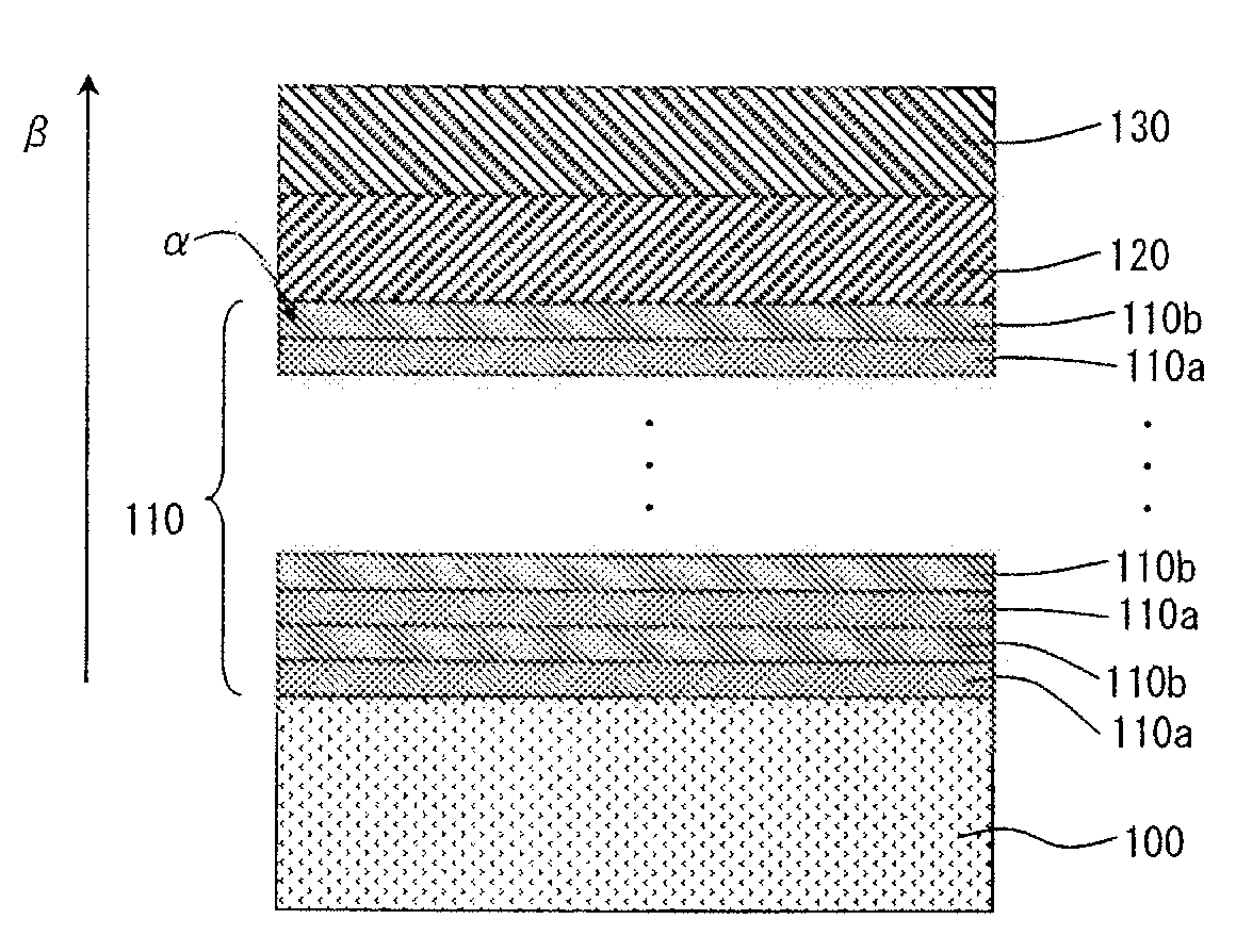
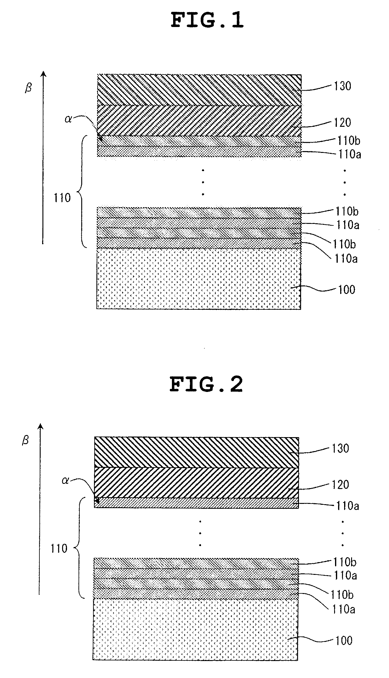
[0047]FIGS. 1 and 2 are each a sectional view illustrating a compound semiconductor substrate according to a first embodiment of the invention.

[0048]As illustrated in FIGS. 1 and 2, the compound semiconductor substrate according to the present embodiment has a structure which are successively formed a first intermediate layer 110, a second intermediate layer 120 and a compound semiconductor single crystal layer 130 on a Si single crystal substrate 100.

[0049]The Si single crystal substrate 100 is a Si single crystal substrate having a surface having a crystal plane orientation of a {111} plane. The plane orientation {111} may be a fine inclination (about more than ten degrees) of any normal crystal plane orientation {111}, or any one of crystal plane orientations having higher-order Miller indices, such as {211}. When the crystal plane orientation of the surface of the Si single crystal substrate 100 is made into {111} in this way, the generation of anti-phase boundary defects is dec...

second embodiment

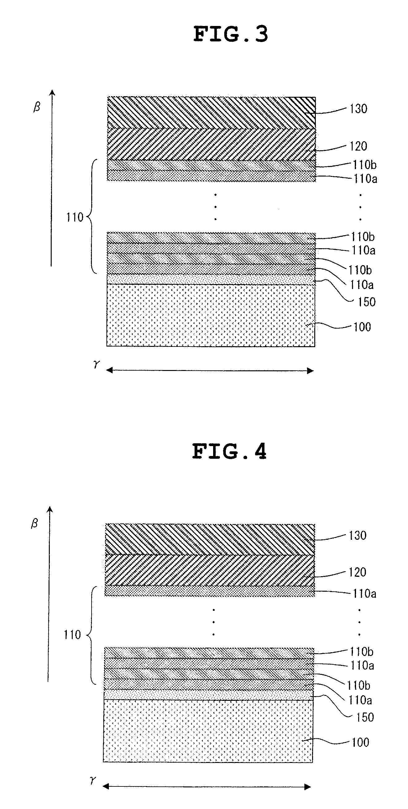
[0083]FIGS. 3 and 4 are each a sectional view illustrating a compound semiconductor substrate according to a second embodiment of the invention.

[0084]The compound semiconductor substrate according to the embodiment is different from the first embodiment in that a 3C—SiC single crystal layer 150 is formed between the first intermediate layer 110 and the Si single crystal substrate 100. Since the others are the same as in the first embodiment, description thereof is omitted.

[0085]Specifically, as illustrated in FIGS. 3 and 4, in the compound semiconductor substrate according to the embodiment, the 3C—SiC single crystal layer 150 is formed on the Si single crystal substrate, which has a crystal plane orientation of a {111} plane, and further the same first intermediate layer 110 as described in the first embodiment is formed on the 3C—SiC single crystal layer 150.

[0086]The film thickness of the 3C—SiC single crystal layer 150 preferably ranges from 10 to 800 nm. If the film thickness i...

third embodiment

[0089]FIGS. 5 and 6 are each a sectional view illustrating a compound semiconductor substrate according to a third embodiment of the invention.

[0090]As illustrated in FIGS. 5 and 6, the compound semiconductor substrate according to the present embodiment has a structure which are successively formed a first intermediate layer 210, a second intermediate layer 220 and a compound semiconductor single crystal layer 230 on a Si single crystal substrate 200.

[0091]The Si single crystal substrate 200 may be identical to the Si single crystal substrate 100 described about the first embodiment.

[0092]As illustrated in FIG. 5 or 6, in the first intermediate layer 210, a 3C—SiC single crystal layer 210a and a metal compound layer 210b are laminated, over the Si single crystal substrate 200, in this order repeatedly so as to alternate the resultant 3C—SiC single crystal layers 210a with the resultant metal compound layers 210b and render the topmost layer α of the laminate one of the 3C—SiC singl...


PUM


Abstract

Provides is a compound semiconductor substrate about which the thickness of its nitride semiconductor single crystal layer can be made large while the generation of cracks, crystal defects or the like is restrained in the nitride semiconductor single crystal layer. The substrate has a first intermediate layer 110 formed on a Si single crystal substrate 100 having a crystal plane orientation of {111}. In the layer 110, a first metal compound layer 110a made of any one of TiC, TiN, VC and VN, and a second metal compound layer 110b made of any one of compounds which are different from the compound of the first metal compound layer out of TiC, TiN, VC and VN are laminated in this order alternately each other over the Si single crystal.

Description

BACKGROUND OF THE INVENTION[0001]1. Field of the Invention[0002]The present invention relates to a compound semiconductor substrate used preferably for a light emitting device or an electronic device.[0003]2. Description of the Related Art[0004]Nitride semiconductors, typical examples of which include gallium nitride (GaN) and aluminum nitride (AlN), have been expected to be applied to light emitting devices, electronic devices which can be operated at a high speed and at a high temperature, and other devices since the semiconductors have excellent properties such as high electron mobility and high heat resistance.[0005]Conventionally, for a substrate which constitutes such a nitride semiconductor, sapphire, silicon (Si), zinc oxide (ZnO) and so on have been used. In these substrates, a Si single crystal substrate is better in crystallinity and can be produced into a larger area with a higher purity at lower costs than other substrates. Thus, the single crystal substrate is preferab...

Claims


Application Information

Patent Timeline
IPC IPC(8): H01L29/205
CPCC30B25/02C30B25/18C30B29/403H01L21/02381H01L21/02447H01L33/007H01L21/02488H01L21/02491H01L21/02505H01L21/0254H01L21/02458
Inventor ABE, YOSHIHISAKOMIYAMA, JUNSUZUKI, SHUNICHIOISHI, HIROSHIYOSHIDA, AKIRANAKANISHI, HIDEO
Owner COVALENT MATERIALS CORP
Learn More