Measuring etching rates using low coherence interferometry

a low coherence interferometer and etching rate technology, applied in the direction of fluid pressure measurement, semiconductor/solid-state device testing/measurement, instruments, etc., can solve the problems of complex measurement process, many sensors and mems devices required, device failure,

Inactive Publication Date: 2009-03-12
EASTMAN KODAK CO
View PDF8 Cites 22 Cited by
  • Summary
  • Abstract
  • Description
  • Claims
  • Application Information

AI Technical Summary

Benefits of technology

[0019]As a further advantage, the method of the present invention allows real-time monitoring of the etching rate, useful in a control loop that regulates the etch rate.

Problems solved by technology

Moreover, many sensors and MEMS devices are required to operate in harsh chemical environments.
In these cases, etching of the materials used in the sensors by the chemical environment can lead to device failure.
There are inherent difficulties that complicate the measurement process in etching processes that make some conventional approaches unworkable for in situ measurement.
However, quartz crystal microbalance methods like this require that the material to be etched be first coated on the quartz crystal.
This is not convenient and limits the application of this method to materials from which suitable coatings on the quartz crystal monitor can be made.
Even for materials, which can be coated, the quartz crystal microbalance technique is limited to coatings, which can be prepared in the operating range of the quartz crystal, that is temperatures below 570° C.
It is also inconvenient because in practice this method requires electrical contacts to be made on the material, such as by vacuum deposition of a metal on a surface of the material to be etched.
Furthermore, this method requires use of a reference electrode, which can limit the usefulness of this method.
Both of these techniques are limited to front side applications.
This technique does not measure etching rates and the requirement for a reference sample limits its scope of applicability.
However this requires adding a tracking agent to the etchant and the method is inherently indirect.
Surface roughness on the sample will greatly affect the results of this type of measurement and it is limited in resolution to about 0.1 μm.
In some cases this is undesirable since it can complicate the etching set-up and adds cost.
Moreover, these spectroscopic techniques are limited in their application to optically transparent etching environments.
Profilometry is not suitable for in situ measurements because it requires removal and manipulation of the sample.
However, such a solution requires space in the etching environment, requires an interface for its removal and reinsertion, introduces additional surface area and waste, and necessitates time delay so that the ability to obtain dynamic measurement data is compromised.

Method used


Image

  • Measuring etching rates using low coherence interferometry
  • Measuring etching rates using low coherence interferometry
  • Measuring etching rates using low coherence interferometry

Examples


example 1

[0072]This example shows the effect of temperature on optical thickness measured by low coherence interferometry using the apparatus described in FIG. 8. FIG. 11 shows a graph of measured optical thickness as a function of temperature for a 26.6 mm on a side square coupon (709.7 sq mm) of silicon mounted in the fixture shown in FIGS. 6 and 7. The temperature ramp was 10° C. per hour. The fit of the data shown in FIG. 11 was obtained from a regression analysis of the raw data using the relationship shown in equation (17). The best fit data is n=3.49749, to=694.420 μm, α=4.15E-06 / K and dn / dT=2.37E-04 / K where to is the initial thickness. Since the thermo optic coefficient of silicon is approximately 2 orders of magnitude larger than typical glass substrates when determining etching rates of silicon it is desirable to measure temperature along with thickness to study dissolution effects in real time using low-coherence interferometry.

example 2

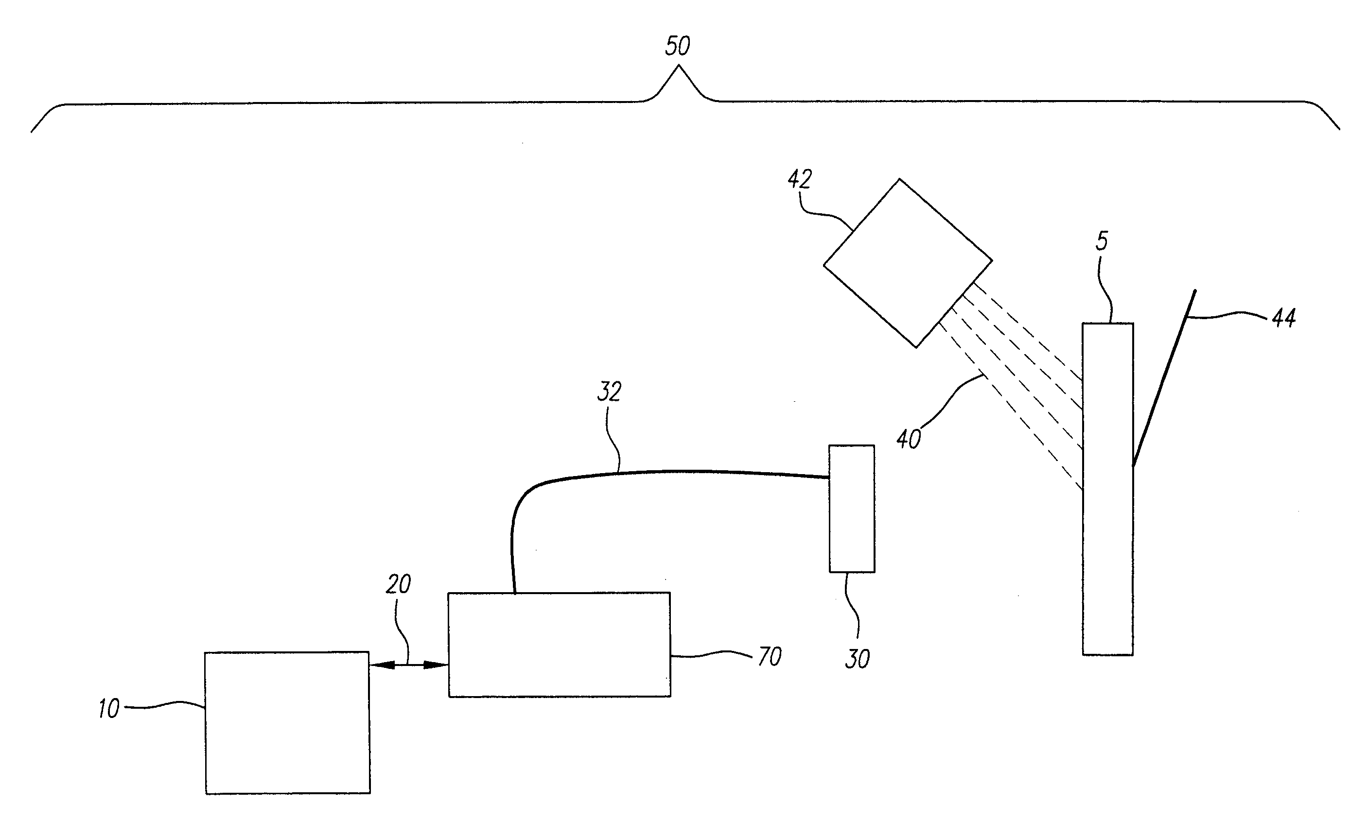
[0073]This example shows how low coherence interferometry has been implemented to measure in situ etch rates for a homogeneous material, in this case silicon. A silicon coupon in the 100-orientation (Si(100)) (709.7 sq mm, 0.35 mm thick) polished on both sides was mounted in the fixture shown in FIG. 6, with the fixture mounted in an oven. The position (lateral, vertical, and angular) of the interferometric probe (30 in FIG. 6) was adjusted to obtain signals from the optical interfaces of the silicon. The etching solution (pH 10 buffer obtained from Ricca Chemical Co., experimental pH 10.06) was supplied from a reservoir of etching solution suspended in a constant temperature bath. A recirculation system was used to introduce the etchant into the etching chamber. The recirculation system was comprised of PTFE and stainless steel tubing, a pump and controller, needle valves to regulate pressure and flow, and pressure gauges. In this experiment, the pressure was maintained at atmosphe...

example 3

[0074]This example shows how low coherence interferometry can be used to measure in situ etch rates for a homogeneous material, in this case borosilicate glass. A borosilicate glass coupon (709.7 sq mm, 1.1 mm thick) was mounted the fixture shown in FIG. 6. The etchant was Kodak 1015 Flush Fluid (1015 FF) solution (pH 11.3). Using the recirculation system described in Example 2, the pressure was set to 25 psi, and the temperature of the etching environment was adjusted to 71.0° C. The progress of etching of the borosilicate glass was followed by low coherence interferometry. The optical thickness measurements are shown in FIG. 13. From a linear fit of the in situ monitoring of the optical thickness (fit shown in FIG. 13, slope=23.7 optical nm / h) divided by the refractive index of the glass (1.46), the etch rate was determined to be 16.2 nm / h. After exposure to the etchant for 21.5 h, the borosilicate glass coupon was analyzed by profilometry at the boundary between the glass surface...


PUM

PropertyMeasurementUnit
temperaturesaaaaaaaaaa
pHaaaaaaaaaa
coherence lengthaaaaaaaaaa

Abstract

Measuring thickness and the rate of change of thickness of a material having a surface while the material is being etched, comprising: illuminating the material with low coherence light, a portion of the which transmits through the material and a portion of which is reflected; etching the material surface and while etching, collecting a portion of the reflected light from each optical interface of the material with a low coherence light interferometer; calculating the thickness and rate of change of thickness of the material or part of the material according to the obtained interferometric data; and storing or displaying the resultant thickness and rate of change of thickness of the material. The present invention provides a unique way of calculating the thermo optic coefficient of a material. This method can be used simultaneously with etching the material so that changes to the etching rate can be made in real time.

Description

CROSS REFERENCE TO RELATED APPLICATIONS[0001]The present application is related to U.S. Ser. No. 11 / 262,868, filed Oct. 31, 2005, by Michael Alan Marcus et al., entitled “Measuring Layer Thickness Or Composition Changes”.FIELD OF THE INVENTION[0002]The present invention relates to providing physical measurements of the thickness of a material and more particularly relates to measuring the thickness and rate of etching, and composition of such etched material while the material is being etched.BACKGROUND OF THE INVENTION[0003]Many micro-electromechanical systems (MEMS) devices, sensors, integrated circuits, and optical and electro-optical elements require controlled removal of materials such as silicon and silicon oxides. A range of etching processes, including dry and wet etching processes, can be used to remove material to produce patterns or useful features. Moreover, many sensors and MEMS devices are required to operate in harsh chemical environments. In these cases, etching of t...

Claims


Application Information

Patent Timeline
Patent Type & Authority Applications(United States)
IPC IPC(8): C03C15/00
CPCG01B11/0675H01L22/26H01L22/12
Inventor DOCKERY, KEVIN P.MARCUS, MICHAEL A.SIEBER, KURT D.
Owner EASTMAN KODAK CO
Why Eureka
Try Eureka